A low-temperature bonding method based on au/in isothermal solidification

A low-temperature bonding and isothermal technology, applied in semiconductor/solid-state device manufacturing, electrical solid-state devices, semiconductor devices, etc., can solve the problem that surface-activated low-temperature bonding is difficult to meet the requirements of graphics circuits and wafer bonding, and increases the difficulty of the process. Process costs, the flatness of the surface to be bonded and other issues, to achieve the effect of strong plasticity, reduced bonding alignment accuracy, and low cost

Active Publication Date: 2019-08-02
SUZHOU INST OF NANO TECH & NANO BIONICS CHINESE ACEDEMY OF SCI
View PDF8 Cites 0 Cited by
  • Summary
  • Abstract
  • Description
  • Claims
  • Application Information

AI Technical Summary

Problems solved by technology

[0009] 1. Susceptible to the limitations of the materials to be bonded
For example, anodic bonding requires the migration of sodium ions during the bonding process, which can only be used for silicon-glass bonding, and surface-activated low-temperature bonding, usually only for direct bonding between silicon-silicon
[0010] 2. The temperature during low temperature bonding, that is, the temperature range that the bonding interface can withstand is small
[0011] 3. It is easy to be limited by the flatness of the surface to be bonded
For example, anode bonding, Au / Si eutectic bonding, silicon-silicon bonding, etc., the flatness of the bonding surface is usually required to be less than 1 μm, which greatly increases the difficulty and cost of the process
[0012] 4. Not easy to graph
For example, surface-activated low-temperature bonding is difficult to meet the requirements of patterned circuits and wafer bonding
[0013] 5. Higher requirements for bonding alignment accuracy

Method used


Image

  • A low-temperature bonding method based on au/in isothermal solidification
  • A low-temperature bonding method based on au/in isothermal solidification
  • A low-temperature bonding method based on au/in isothermal solidification

Examples


Embodiment Construction

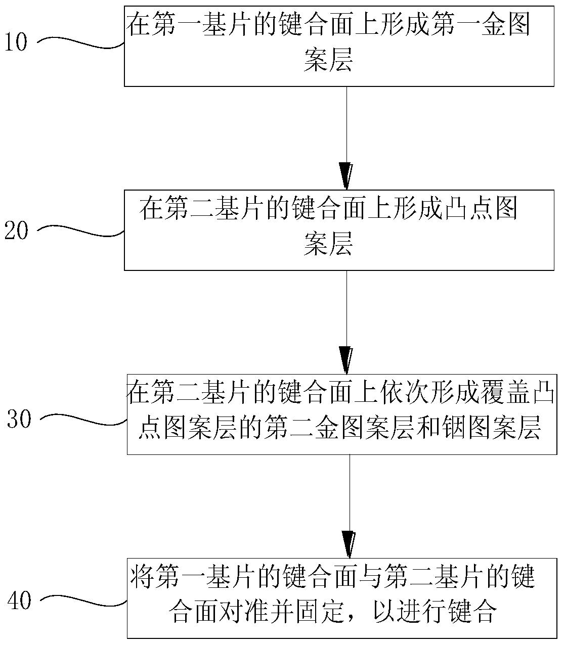
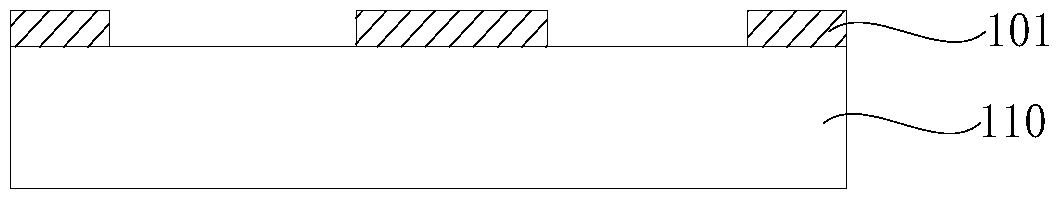
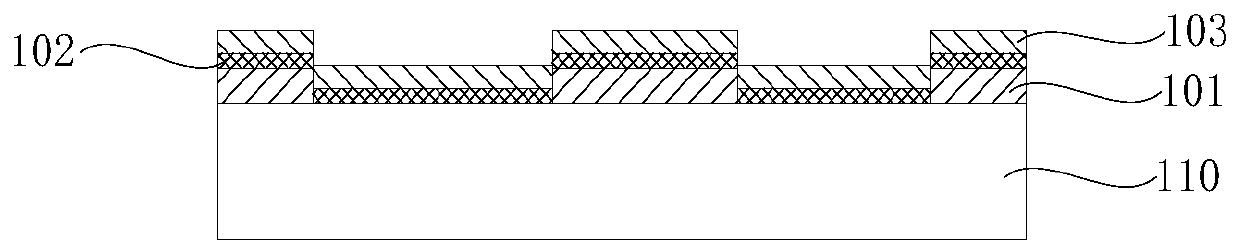
[0035] Hereinafter, embodiments of the present invention will be described in detail with reference to the accompanying drawings. This invention may, however, be embodied in many different forms and should not be construed as limited to the specific embodiments set forth herein. Rather, the embodiments are provided to explain the principles of the invention and its practical application, thereby enabling others skilled in the art to understand the invention for various embodiments and with various modifications as are suited to particular intended uses. In the drawings, the thicknesses of layers and regions are exaggerated for clarity of devices, and the same reference numerals will be used to refer to the same elements throughout the specification and drawings.

[0036] The isothermal solidification process is a liquid / solid interdiffusion and reaction process. In this process, a low-melting point element and a high-melting point element react and diffuse at a slightly highe...


PUM

PropertyMeasurementUnit
depthaaaaaaaaaa

Abstract

The invention discloses a low-temperature bonding method based on Au / In isothermal solidification, comprising: forming a first gold pattern layer on a bonding surface of a first substrate; forming a bump pattern on a bonding surface of a second substrate layer; on the bonding surface of the second substrate, the second gold pattern layer and the indium pattern layer covering the bump pattern layer are sequentially formed; the bonding surface of the first substrate is bonded to the second substrate Align and secure the bonding surfaces for bonding. The present invention uses a raised dot pattern layer on the bottom layer of the metal film. The raised dot pattern layer not only reduces the bonding alignment accuracy, but also enhances the contact force in the bonding process, which can greatly improve the bonding quality.

Description

technical field [0001] The invention relates to a low-temperature bonding method based on Au / In isothermal solidification. Background technique [0002] Bonding technology refers to the technology in which two silicon wafers are attracted to each other by the van der Waals force at room temperature, and the surface groups of the silicon wafers undergo chemical interactions to bond together, which can combine surface silicon processing and bulk silicon processing. Organically combined is an important processing method in MEMS (micro-electromechanical systems) technology. The use of bonding technology can reduce the complexity of single silicon wafer processing, so as to realize complex communication, cavity and SOI (silicon on insulator) material preparation, etc. In addition, bonding technology can also realize the permanent connection of components of different materials in MEMS devices, so as to realize three-dimensional integration and wafer-level packaging of chips. ...

Claims


Application Information

Patent Timeline
Patent Type & Authority Patents(China)
IPC IPC(8): H01L21/60
CPCH01L24/11H01L24/81H01L2224/11614H01L2224/145H01L2224/81895H01L2924/01079H01L2924/01049H01L2224/11
Inventor 沈文江
Owner SUZHOU INST OF NANO TECH & NANO BIONICS CHINESE ACEDEMY OF SCI
Why Eureka
Try Eureka