Pattern electroplating method for microstrip circuit

A graphic electroplating and microstrip circuit technology, applied in the direction of circuits, electrical components, electrical solid devices, etc., can solve the problems of electroplating deposition of functional layers in non-graphic areas, warping of electroplating functional layers, difficulty in controlling the adhesion of circuit film layers, etc. Achieve the effects of improving the cutting quality and yield, reducing the electroplating coating area, and reducing the phenomenon of film peeling off

Inactive Publication Date: 2017-01-04
THE 41ST INST OF CHINA ELECTRONICS TECH GRP
View PDF3 Cites 18 Cited by
  • Summary
  • Abstract
  • Description
  • Claims
  • Application Information

AI Technical Summary

Problems solved by technology

[0003] Because the electroplating layer itself has a certain stress, coupled with the electroplating functional layer and protective layer on the back of the entire board, the two processes of loading and releasing the protective layer have a major impact on the stress of the electroplating functional layer, resulting in cutting circuits, especially along the The electroplating functional layer often warps and falls off on both sides of the dicing track on the back of the substrate, which makes it difficult to control the adhesion of the circuit film layer, and also causes electroplating deposition of the functional layer in the non-graphic area on the back
This method not only affects the performance and yield of thin film circuits, but also causes a certain waste of precious metals.

Method used


Image

  • Pattern electroplating method for microstrip circuit
  • Pattern electroplating method for microstrip circuit
  • Pattern electroplating method for microstrip circuit

Examples


Embodiment Construction

[0046] Below in conjunction with accompanying drawing and specific embodiment the present invention is described in further detail:

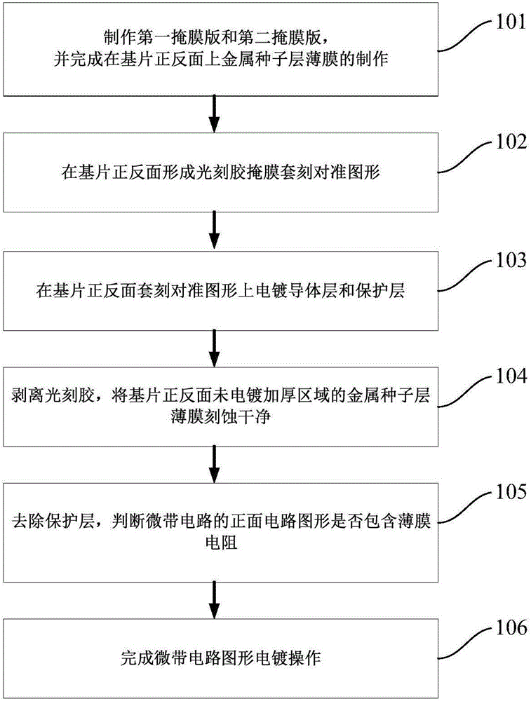
[0047] A method for pattern electroplating of microstrip circuits (such as figure 1 shown), follow the steps below:

[0048] Step 101: Use the front conductor pattern on the circuit, the scribe mark and the front alignment mark as the first information layer to make a first mask, and use the back conductor pattern and the back alignment mark on the circuit as the second information layer Making the second mask plate, and completing the making of the metal seed layer film on the front and back of the substrate.

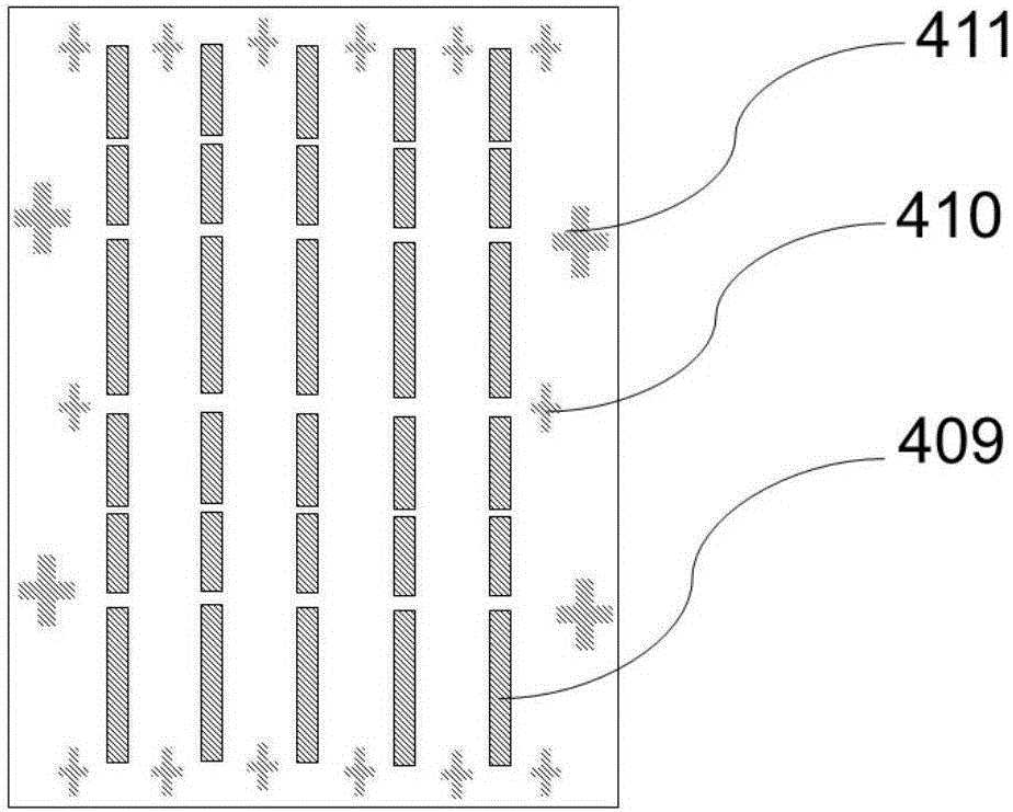
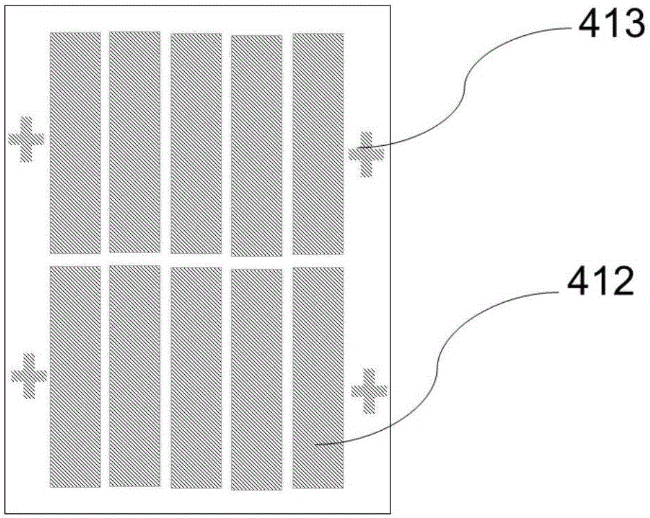
[0049] Specifically: use the front conductor pattern 409 of the circuit, the scribe mark 410 and the front alignment mark 411 as the first information layer to make the first mask (such as Figure 2a As shown), the reverse conductor pattern 412 and the reverse alignment mark 413 are used as the second information layer to make a second...


PUM


Abstract

The invention discloses a pattern electroplating method for a microstrip circuit, wherein the pattern electroplating method belongs to the technical field of a microwave millimeter wave film mixed integrated circuit. According to the pattern electroplating method, in the microstrip circuit with relatively large number of isolated conductor patterns, an original method of combining substrate front-surface pattern electroplating and back ground-surface integral electroplating is changed to a double-surface pattern electroplating process so that a medium layer at a cutting channel position is exposed to outside, thereby effectively preventing film layer falling in cutting the microstrip circuit, improving cutting quality and yield rate of the microstrip circuit, and settling a problem of film layer warpage and falling caused by stress influence to an electroplating functional layer of the microstrip circuit in a loading process and a discharging process of the electroplating protecting layer on the cutting channel in manufacture according to an existing process. According to the pattern electroplating method, electroplating deposition of the functional layer is only performed on the conductor pattern areas on the front surface and the back surface of an array circuit, thereby preventing plating of noble metals such as gold on other areas such as cutting channels and process edges outside the array pattern, reducing electroplating area and saving cost.

Description

technical field [0001] The invention belongs to the technical field of microwave and millimeter wave thin film hybrid integrated circuits, and in particular relates to a pattern electroplating method for microstrip circuits. Background technique [0002] Pattern plating, also known as tape plating or photoresist mask plating, has the advantages of small conductor pattern side growth, steep line edges, and high pattern resolution, and is widely used in the production of microstrip circuits. The current microstrip circuit pattern electroplating method usually uses the pattern electroplating method for the front circuit, that is, on the basis of vacuum coating, first use the reverse plate to make a photoresist mask, except for the required pattern exposure, the rest Cover with a photoresist mask, and then rely on the metal seed layer under the photoresist to do electrical connection of the pattern for electroplating to prepare the functional layer and protective layer. Layer, ...

Claims


Application Information

Patent Timeline
Patent Type & Authority Applications(China)
IPC IPC(8): H01L21/70H01L27/01
CPCH01L21/707H01L27/016
Inventor 曹乾涛龙江华赵海轮
Owner THE 41ST INST OF CHINA ELECTRONICS TECH GRP
Why Eureka
Try Eureka