Method of manufacturing field effect transistor without contact holes and field effect transistor without contact holes

A technology of field effect tubes and manufacturing methods, which is applied in the field of field effect tubes without contact holes, and can solve the problems of limiting the integration of field effect tubes and not being too close

Inactive Publication Date: 2017-01-04
PEKING UNIV FOUNDER GRP CO LTD +1
View PDF4 Cites 3 Cited by
  • Summary
  • Abstract
  • Description
  • Claims
  • Application Information

AI Technical Summary

Problems solved by technology

The above two factors (the edge of the contact hole cannot be too close to the trench, and the opening size of the contact hole itself cannot be too small) determine that the distance between two adjacent deep trenches cannot be too close, which limits the field effect transistor. Integration

Method used


Image

  • Method of manufacturing field effect transistor without contact holes and field effect transistor without contact holes
  • Method of manufacturing field effect transistor without contact holes and field effect transistor without contact holes
  • Method of manufacturing field effect transistor without contact holes and field effect transistor without contact holes

Examples


Embodiment Construction

[0028] In order to have a clearer understanding of the above objects, features and advantages of the present invention, the present invention will be further described in detail below in conjunction with the accompanying drawings and specific embodiments. It should be noted that, in the case of no conflict, the embodiments of the present application and the features in the embodiments can be combined with each other.

[0029] In the following description, many specific details are set forth in order to fully understand the present invention. However, the present invention can also be implemented in other ways different from those described here. Therefore, the protection scope of the present invention is not limited by the specific details disclosed below. EXAMPLE LIMITATIONS.

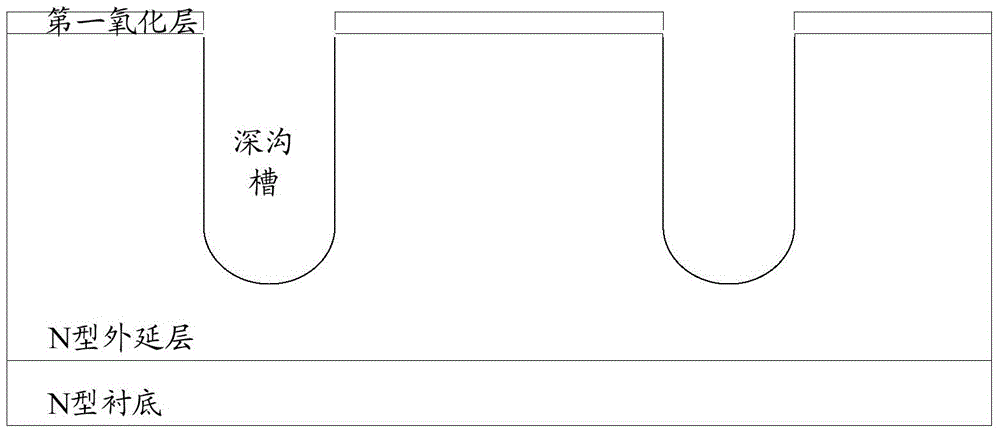
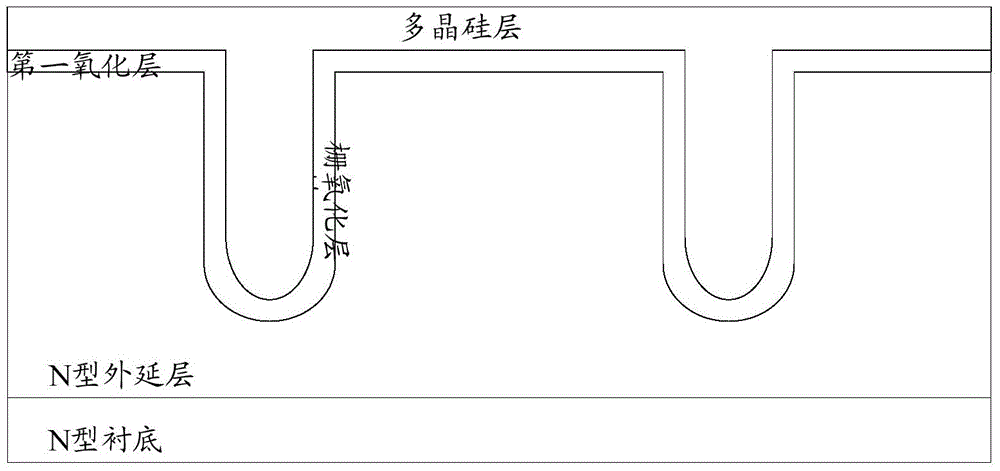
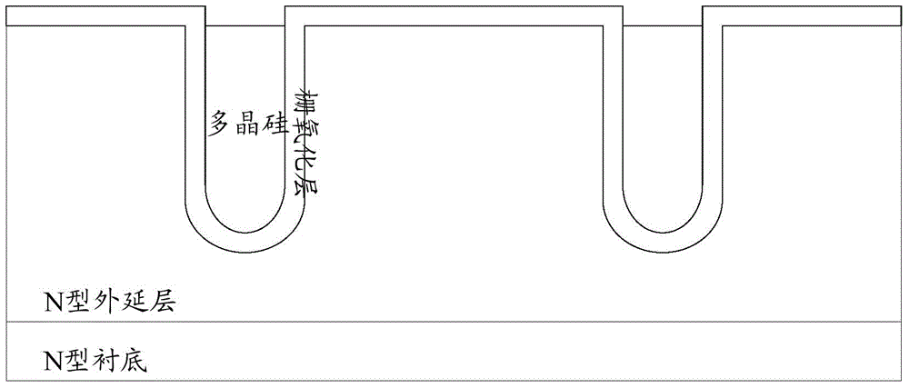
[0030] Figure 8 A schematic flowchart showing a method for manufacturing a field effect transistor without a contact hole according to an embodiment of the present invention.

[0031] Such as Figu...


PUM

PropertyMeasurementUnit
Thicknessaaaaaaaaaa

Abstract

The invention proposes a method of manufacturing a field effect transistor without contact holes and a field effect transistor without contact holes. The method comprises the following steps: growing an epitaxial layer on a substrate, and growing a first oxide layer on the epitaxial layer; etching multiple deep trenches on the first oxide layer and the epitaxial layer; growing a second oxide layer in each deep trench of the multiple deep trenches; growing a silicon nitride layer on the first oxide layer and the second oxide layer; growing a polycrystalline silicon layer on the silicon nitride layer of the first oxide layer and the second oxide layer; etching all of the polycrystalline silicon layer on the silicon nitride layer of the first oxide layer and part of the polycrystalline silicon layer on the silicon nitride layer of the second oxide layer; growing a third oxide layer on the rest of the polycrystalline silicon layer; and etching the silicon nitride layer on the first oxide layer and the first oxide layer. Through the technical scheme of the invention, the influence of the distance between contact holes and deep trenches and the metal in the contact holes on the degree of integration of the field effect transistor is avoided, and a high degree of integration of the field effect transistor is ensured.

Description

technical field [0001] The invention relates to the technical field of semiconductors, in particular to a method for manufacturing a field effect transistor without a contact hole and a field effect transistor without a contact hole. Background technique [0002] When manufacturing super junction conventional trench VDMOS (Vertical-Doublediffused-Metal-Oxide-Semiconductor-Field-Effect-Transistor, vertical double-diffused metal-oxide-semiconductor structure), a current practice is, as Figure 1 to Figure 7 shown, including the following steps: making deep trenches (such as figure 1 shown); growing gate oxide and polysilicon (eg figure 2 shown); etching polysilicon (such as image 3 as shown); making body regions (such as Figure 4 as shown); make the source area (such as Figure 5 shown); growing the dielectric layer and making contact holes (such as Figure 6 as shown); making the metal layer (such as Figure 7 shown). [0003] However, when lithography is performed ...

Claims


Application Information

Patent Timeline
IPC IPC(8): H01L29/78H01L21/336H01L21/311
CPCH01L29/7802H01L21/31105H01L29/66712
Inventor 马万里李理赵圣哲
Owner PEKING UNIV FOUNDER GRP CO LTD
Why Eureka
Try Eureka