LDMOS (laterally diffused metal oxide semiconductor) field effect transistor with bulk electric field modulation function

An oxide semiconductor and lateral double-diffusion technology, which is applied in semiconductor devices, semiconductor/solid-state device manufacturing, circuits, etc., can solve problems such as device breakdown at the drain terminal, device performance limitations, breakdown, etc., and achieve breakdown voltage The effect of improving and improving the performance of the device

Active Publication Date: 2017-01-04
XIDIAN UNIV
View PDF3 Cites 6 Cited by
  • Summary
  • Abstract
  • Description
  • Claims
  • Application Information

AI Technical Summary

Problems solved by technology

[0003] However, experiments have shown that these improved devices are prone to breakdown in the drain body
After analyzing the reasons, the applicant believes that the body electric field of LDMOS has not been optimized, so that a p

Method used


Image

  • LDMOS (laterally diffused metal oxide semiconductor) field effect transistor with bulk electric field modulation function

Examples


Embodiment Construction

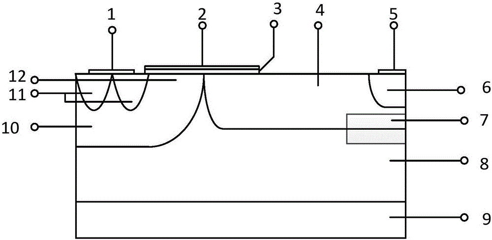
[0036] Such as figure 1 As shown, the lateral double-diffused MOSFET structure of the present invention includes:

[0037] a substrate 9 of semiconductor material;

[0038] an epitaxial layer 8 on the substrate and form a SiC buried layer 7;

[0039] The base region 10 and the drain region 6 respectively located at both ends of the epitaxial layer, and the drain region 5 above the drain region;

[0040] source region 11 and channel 12 located on the surface of the base region;

[0041] The source electrode 1 is formed on the surface of the source region, and the gate insulating layer 3 is located below the gate 2 on the channel 12;

[0042] The drift region 4 is between the channel and the drain region;

[0043] A wide bandgap semiconductor SiC buried layer is formed under the drain terminal of the LDMOS device by heteroepitaxial technology. On the one hand, the breakdown position of the device is formed in the SiC material with a high critical breakdown electric field. T...


PUM

PropertyMeasurementUnit
Thicknessaaaaaaaaaa
Doping concentrationaaaaaaaaaa

Abstract

The invention provides an LDMOS (laterally diffused metal oxide semiconductor) field effect transistor with a bulk electric field modulation function. The LDMOS field effect transistor has the characteristic that a wide bandgap semiconductor SiC (silicon carbide) burying layer is formed under the drain end of the LDMOS field effect transistor by a heteroepitaxy technique; an internal high peak electric field under the drain end is led into the SiC burying layer, the characteristic of higher critical breakdown electric field (EC-SiC=3.0*106V/cm greater than EC-Si=3.0*105V/cm) of the SiC material is utilized, and the breakdown occurs in the SiC burying layer, so that the breakdown voltage of the LDMOS is effectively increased, and the property of the LDMOS field effect transistor is greatly improved.

Description

technical field [0001] The invention relates to the field of semiconductor devices, in particular to a lateral double-diffused metal oxide semiconductor field effect transistor. Background technique [0002] In the power monolithic integration technology, combined with isolation technology and high-voltage and low-voltage compatibility and other key processes, the integrated high-voltage power device is the core of the power integrated circuit (PIC). Due to the advantages of lateral double-diffused MOS (LDMOS) devices in terms of easy integration, good frequency characteristics, and low power consumption, LDMOS has been used as a key core device in high-voltage power integrated circuits (HVIC) and smart power integrated circuits (SPIC). In recent years, with the continuous development of power electronics, low-cost and high-reliability requirements have been put forward for core power devices such as lateral double-diffused MOS devices (ie, LDMOS). The field plate technolog...

Claims


Application Information

Patent Timeline
IPC IPC(8): H01L29/78H01L21/336
CPCH01L29/66681H01L29/7816
Inventor 段宝兴曹震吕建梅董自明师通通杨银堂
Owner XIDIAN UNIV
Why Eureka
Try Eureka