Film packaging structure, preparation method and organic light emitting apparatus with same
A thin-film encapsulation and thin-film technology, which is used in the manufacture of semiconductor/solid-state devices, electrical components, and electrical solid-state devices, etc., can solve the problems of poor water and oxygen barrier properties and unsatisfactory flexibility, and achieve good water and oxygen barrier properties, suitable for The effect of mass production and easy packaging process
- Summary
- Abstract
- Description
- Claims
- Application Information
AI Technical Summary
Problems solved by technology
Method used
Image


Examples
preparation example Construction
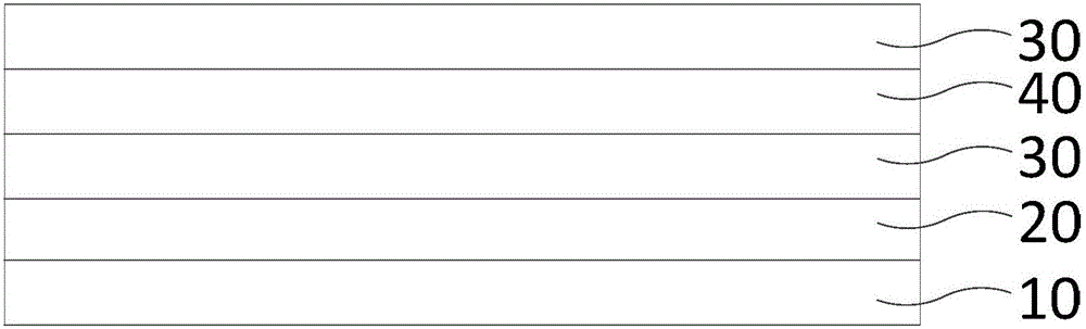
[0052] Taking the encapsulation of OLED devices as an example, the exemplary preparation method of the thin film encapsulation structure of the present invention includes the following steps:
[0053] (1) Place the OLED device on one side of the substrate 10 in a sputtering chamber, and prepare an inorganic layer thin film 30 by sputtering against a target, and the thickness of the film layer is 5-2000 nm;
[0054] (2) preparing an organic layer film 40 on the inorganic layer film 30 of the OLED device, with a film thickness of 50 nm to 15 μm;
[0055] (3) Steps (1) and (2) are repeated to prepare alternately stacked inorganic layer films 30 and organic layer films 40, and the lowermost and uppermost layers are inorganic layer films 30, and the thickness of the formed thin film packaging structure is 100nm~50μm.
[0056] The thin film encapsulation structure formed by the alternate lamination of the above-mentioned inorganic layer films 30 and organic layer films 40 has strong...
Embodiment 1
[0057] Example 1: Alumina-zirconia / acrylic thin film encapsulation structure
[0058] 1) Place the OLED device on one side of the substrate 10 in a sputtering chamber. The first target 60 and the second target 70 are high-purity aluminum targets and zirconium targets respectively, and the reactive gas oxygen is introduced into the sputtering chamber by sputtering the target. Inorganic layer thin film 30 is prepared by irradiation method, and the film thickness is about 500nm;
[0059] (2) Prepare a polyimide film on the inorganic layer film 30 of the OLED device by spin coating, and the film thickness of the organic layer film 40 is about 3 μm;
[0060] (3) Repeat steps (1) and (2) to prepare alternately laminated inorganic layer films 30 and organic layer films 40, the bottom and top layers are inorganic layer films 30, and the number of film layers is 3 layers, forming a film encapsulation structure The thickness is about 4 μm.
Embodiment 2
[0061] Example 2: Alumina-zirconia / acrylic thin film encapsulation structure
[0062] 1) Place the OLED device on one side of the substrate 10 in a sputtering chamber. The first target 60 and the second target 70 are high-purity aluminum targets and zirconium targets respectively, and the reactive gas oxygen is introduced into the sputtering chamber by sputtering the target. The inorganic layer thin film 30 is prepared by irradiation method, and the thickness of the film layer is about 100nm;
[0063] (2) Prepare a polysiloxane-polysilazane film on the inorganic layer film 30 of the OLED device by spraying, and the film thickness of the organic layer film 40 is about 300nm;
[0064] (3) Repeat steps (1) and (2) to prepare alternately stacked inorganic layer films 30 and organic layer films 40, the bottom and top layers are inorganic layer films 30, and the number of film layers is 21 layers, forming a thin film packaging structure The thickness is about 4.1 μm.
PUM
| Property | Measurement | Unit |
|---|---|---|
| thickness | aaaaa | aaaaa |
| thickness | aaaaa | aaaaa |
| thickness | aaaaa | aaaaa |
Abstract
Description
Claims
Application Information
 - R&D
- Intellectual Property
- Life Sciences
- Materials
- Tech Scout
- Unparalleled Data Quality
- Higher Quality Content
- 60% Fewer Hallucinations
Browse by: Latest US Patents, China's latest patents, Technical Efficacy Thesaurus, Application Domain, Technology Topic, Popular Technical Reports.
© 2025 PatSnap. All rights reserved.Legal|Privacy policy|Modern Slavery Act Transparency Statement|Sitemap|About US| Contact US: help@patsnap.com