

Semiconductor laser with internal optical grating
A laser and semiconductor technology, applied in the field of lasers, can solve the problems of large power consumption, large volume, large temperature drift coefficient, etc., to achieve the effect of improving working life, optimizing efficiency, and reducing leakage
- Summary
- Abstract
- Description
- Claims
- Application Information
AI Technical Summary
Problems solved by technology
Method used
Image

Examples
Embodiment Construction
[0033] In order to enable those skilled in the art to better understand the technical solutions in the embodiments of the present invention, and to make the above-mentioned purposes, features and advantages of the embodiments of the present invention more obvious and understandable, the following describes the technical solutions in the embodiments of the present invention in conjunction with the accompanying drawings For further detailed explanation.
[0034] In the description of the present invention, unless otherwise specified and limited, it should be noted that the term "connection" should be understood in a broad sense, for example, it can be a mechanical connection or an electrical connection, or it can be the internal communication of two elements, it can be Directly connected or indirectly connected through an intermediary, those skilled in the art can understand the specific meanings of the above terms according to specific situations.
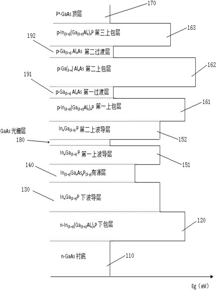
[0035] see figure 1, is a s...
PUM
| Property | Measurement | Unit |
|---|---|---|
| Thickness | aaaaa | aaaaa |
| Thickness | aaaaa | aaaaa |
| Thickness | aaaaa | aaaaa |
Abstract
Description
Claims
Application Information