

Servo control chip SIP system special for chip atomic clock, test device and method
A chip atomic clock and servo control technology, applied in the electronic field, can solve the problems of large volume and power consumption of the atomic clock system, and achieve the effect of reducing the volume and power consumption, reducing the volume and power consumption, and reducing the chip line width
- Summary
- Abstract
- Description
- Claims
- Application Information
AI Technical Summary
Problems solved by technology
Method used
Image

Examples
Embodiment Construction
[0038] In order to make the purpose, technical solution and advantages of the present application clearer, the technical solution of the present application will be clearly and completely described below in conjunction with specific embodiments of the present application and corresponding drawings. Apparently, the described embodiments are only some of the embodiments of the present application, rather than all the embodiments. Based on the embodiments in this application, all other embodiments obtained by persons of ordinary skill in the art without making creative efforts belong to the scope of protection of this application.
[0039] The technical solutions provided by various embodiments of the present application will be described in detail below in conjunction with the accompanying drawings.
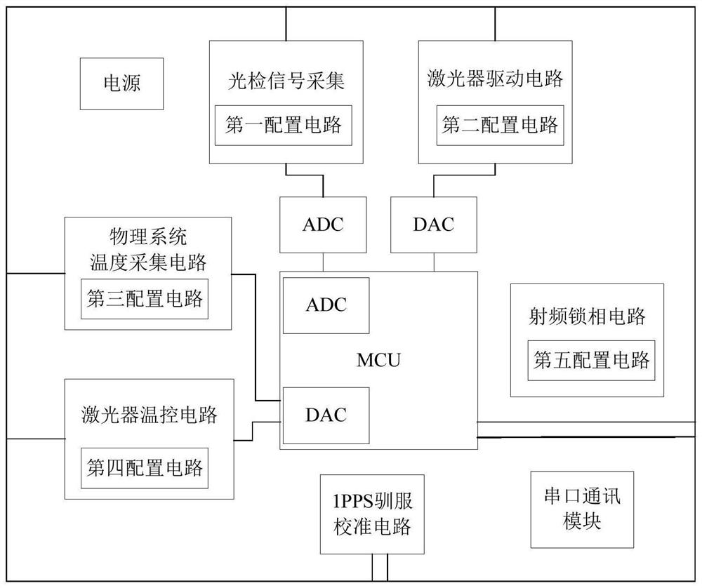
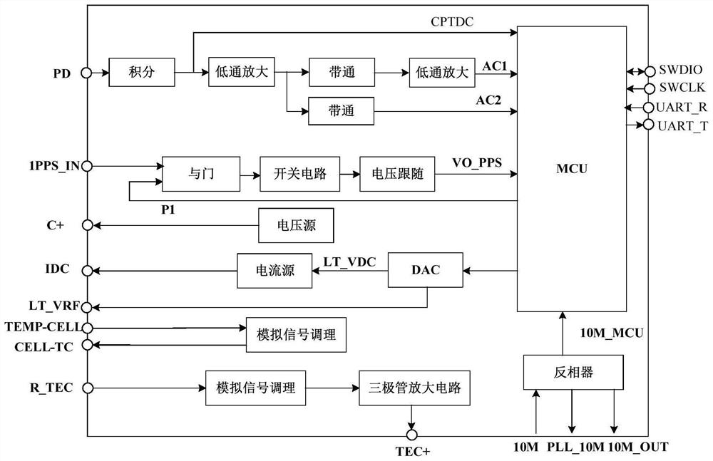
[0040] The invention provides a SIP package scheme of a dedicated servo control chip for a chip atomic clock, and designs a test method suitable for the SIP chip.
[0041] Technic...
PUM
 Abstract
Description
Claims
Application Information