Wafer bonding clamping device, aligning machine, bonding machine and warping substrate adsorption method

A wafer bonding and clamping device technology, which is applied in the manufacture of electrical components, electrical solid devices, semiconductor/solid devices, etc., can solve the problems of unusable warped sheets, delay in production time, complicated operation, etc., and eliminate invalid Pressing surface, improving production efficiency, and uniform heat transfer

Inactive Publication Date: 2017-01-18
SHANGHAI MICRO ELECTRONICS EQUIP (GRP) CO LTD
View PDF8 Cites 24 Cited by
  • Summary
  • Abstract
  • Description
  • Claims
  • Application Information

AI Technical Summary

Problems solved by technology

When the wafer bonding clamping device in the prior art is used to be compatible with substrates of smaller sizes, it is often necessary to replace multiple indenter assemblies. Small area, when replacing wafer substrates of different sizes, it is necessary to change the specifications of the indenter at the same time before it can be used, the operation is more complicated, and the production time is delayed
[0009] 4. The carrier table of the wafer bonding clamping device in the prior art is only equipped with a first-level vacuum adsorption function, and uses the same pressure to absorb the substrate. The carrier table of this structure cannot be used for warped sheets

Method used


Image

  • Wafer bonding clamping device, aligning machine, bonding machine and warping substrate adsorption method
  • Wafer bonding clamping device, aligning machine, bonding machine and warping substrate adsorption method
  • Wafer bonding clamping device, aligning machine, bonding machine and warping substrate adsorption method

Examples


Embodiment 1

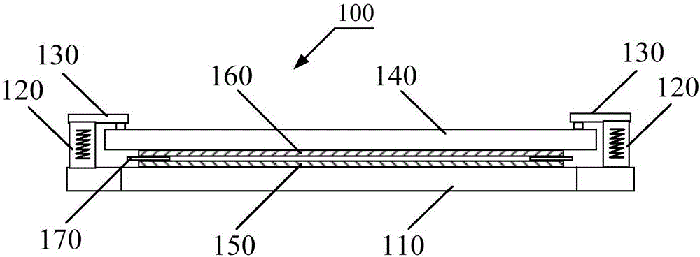
[0054] Such as figure 1 As shown, the first embodiment provides a wafer bonding clamping device 100, which includes a carrying table 110, a clamping mechanism 120, a pressure head 130, and a pressure plate 140. Wherein, the pressure plate 140 is arranged between the carrier 110 and the pressure head 130, the specifications and dimensions of the pressure plate 140 are compatible with the specifications and dimensions of all substrates, and the pressure head 130 is crimped on the pressure plate 140, The pressure head 130 is crimped on the pressure plate 140 and the pressure contact point is set in an area outside the corresponding substrate of the pressure plate 140; the pressure plate 140 is made of the same material as the carrier 110. Among them, the carrying table 110 is used to carry the lower substrate 150 and the upper substrate 160; the clamping mechanism 120 is used to clamp the lower substrate 150 and the upper substrate 160, specifically the clamping mechanism 120 is co...

Embodiment 2

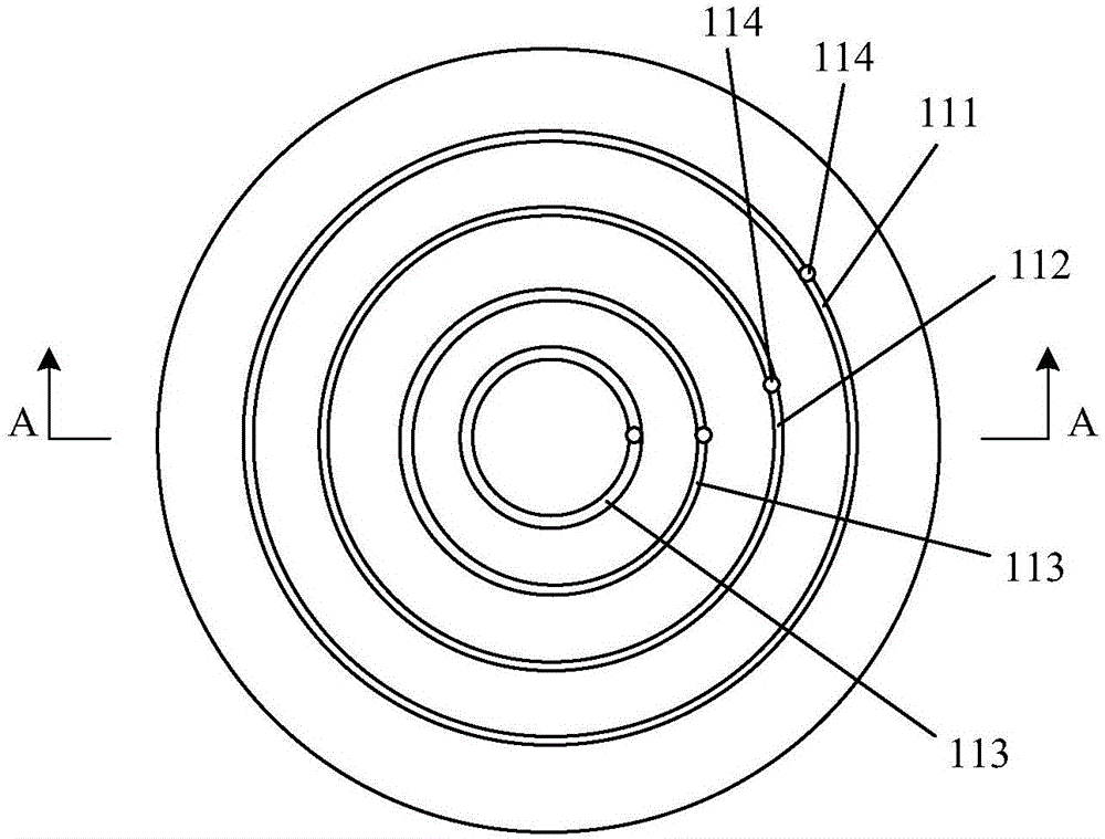
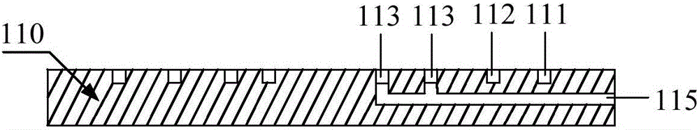
[0059] Such as figure 2 with image 3 As shown, the second embodiment is improved on the basis of the first embodiment. The difference is that the pressure plate 140 and / or the carrying table 110 is provided with a dense-grained suction cup structure. The dense-grained suction cup structure includes several stages of vacuum suction ring grooves arranged in the pressure plate 140 and / or the carrying table 110, and each stage of the vacuum suction ring groove is provided with a vacuum suction hole 114, and each stage has a vacuum suction hole 114. The vacuum adsorption ring groove is connected to the vacuum adsorption hole 114 with a vacuum source of the same or different pressure; the vacuum adsorption hole 114 may also be provided with a switch for controlling the on-off of the vacuum source, the switch may be Solenoid valve or pressure valve or manual valve. At least one vacuum adsorption ring groove is provided in each stage. Among them, the shape of the vacuum suction ring...

Embodiment 3

[0063] Such as Figure 4 with 5 As shown, the third embodiment provides an alignment machine for a wafer bonding system, including a light source 500, an alignment frame 400, a wedge positioning mechanism 300, and a mounting frame 200. The mounting frame 200 has a detachable positive Or, the wafer bonding clamping device 100 of the first or second embodiment described above is installed in the reverse direction.

[0064] In the alignment machine of the third embodiment, the light source accurately aligns the upper and lower substrates through the aligning frame and the wedge-shaped positioning mechanism through the bearing table and the platen 140. The clamping mechanism 120 drives the platen 140 to align the upper and lower substrates. Clamping. Therefore, the present invention also has the effects of reducing or eliminating invalid pressing surfaces, facilitating temperature control, improving production efficiency, and being compatible with all wafer specifications. Figure 4 ...


PUM


Abstract

The invention discloses a wafer bonding clamping device which comprises a loading platform (110), a clamping mechanism (120), a pressing head (130) and a pressing plate (140). The pressing point of the pressing head (130) in the pressing plate (140) is arranged in an area other than the pressing plate (140) corresponding to a substrate. The pressing plate (140) and the loading platform (110) are made of the same material. The pressing plate (140) is compatible with substrates of all sizes. The invention further discloses an aligning machine and a bonding machine, wherein the aligning machine and the bonding machine use the wafer bonding clamping device. According to the invention, ineffective pressing surfaces can be reduced or eliminated, which facilitates temperature control; the production efficiency is improved; the wafer bonding clamping device has the advantages of uniform pressing performance and improves yield, and is compatible with wafers of all sizes and specifications. The invention further discloses a warping substrate adsorption method, so as to realize the adsorption of a warping substrate.

Description

Technical field [0001] The invention relates to the field of semiconductor device equipment manufacturing, in particular to a wafer bonding clamping device, an alignment machine and a bonding machine. Background technique [0002] Wafer bonding technology can bond two wafer substrates together, and the materials of the two wafer substrates can be the same or different. Wafer bonding is an important process for the three-dimensional processing of semiconductor devices. Whether it is anodic bonding, direct bonding, metal extension bonding, metal eutectic bonding and other bonding methods, the main process steps include wafer surface Cleaning and activation processing, wafer alignment, and final wafer bonding steps. Through these process steps, individual single wafers are aligned and then bonded together to achieve their three-dimensional structure. Bonding is not only a packaging technology in microsystem technology, but also an organic part of three-dimensional device manufactu...

Claims


Application Information

Patent Timeline
Patent Type & Authority Applications(China)
IPC IPC(8): H01L21/687H01L21/683H01L21/68H01L21/60
CPCH01L21/681H01L21/6838H01L21/68785H01L24/76H01L2221/683H01L2224/7655
Inventor 江家玮
Owner SHANGHAI MICRO ELECTRONICS EQUIP (GRP) CO LTD
Why Eureka
Try Eureka