Method for manufacturing microbridge of uncooled infrared focal plane detector and structure thereof

A focal plane detector, uncooled infrared technology, applied in the direction of electric radiation detectors, etc., can solve the problems of not too much contribution, no signal response, contribution, etc., to reduce the proportion of invalid absorption, improve absorption efficiency, and improve absorption The effect of proportion

Active Publication Date: 2017-01-25
YANTAI RAYTRON TECH
View PDF5 Cites 37 Cited by
  • Summary
  • Abstract
  • Description
  • Claims
  • Application Information

AI Technical Summary

Problems solved by technology

The incident light radiation is absorbed by the top platform layer and the bottom bridge leg structure, and the infrared radiation absorbed by the bottom bridge leg does not contribute much to the temperature rise of the top platform layer, which leads to the fact that the incident infrared radiation does not really transform into the temperature of the sensitive area. It does not contribute to the signal response, and the response to 12um and smaller pixels is low, which cannot meet the imaging requirements of high-efficiency uncooled infrared detectors

Method used


Image

  • Method for manufacturing microbridge of uncooled infrared focal plane detector and structure thereof
  • Method for manufacturing microbridge of uncooled infrared focal plane detector and structure thereof
  • Method for manufacturing microbridge of uncooled infrared focal plane detector and structure thereof

Examples


Embodiment Construction

[0053] The principles and features of the present invention are described below in conjunction with the accompanying drawings, and the examples given are only used to explain the present invention, and are not intended to limit the scope of the present invention.

[0054] An embodiment of the present invention provides a method for making an uncooled infrared focal plane detector microbridge, see Figure 1 to Figure 8 , its specific process steps are as follows:

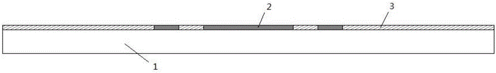
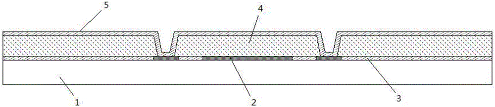
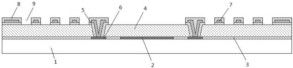
[0055] Such as figure 1 As shown, the reflective layer 2 is made on the wafer with the readout circuit 1 as the base, the material used for the reflective layer 2 is metal, and the thickness of the metal film is The reflection rate of reflective layer 2 metal to infrared light of specific wavelength (such as 8 ~ 14um) is more than 99%. After etching the reflective layer 2, an insulating dielectric layer 3 is deposited on the pattern of the reflective layer 2. The insulating dielectric layer 3 can be made of Si 3 N...


PUM


Abstract

The invention relates to a method for manufacturing microbridge of uncooled infrared focal plane detector and a structure thereof.The method comprises the following steps: preparing a reflecting layer on a readout circuit-based wafer;an insulated medium layer,a first sacrificial layer and a first supporting layer;etching the first supporting layer and preparing a first through hole above the reflecting layer;preparing a fist electrode,a first medium layer,a first passivation layer, a second sacrificial layer,a second supporting layer,a thermal layer and a protective layer;etching the second supporting layer and preparing a second through hole above the first electrode;etching the protective layer and preparing a contact hole above the thermal layer;preparing a second electrode, a second medium layer, a second passivation layer,a third sacrificial layer,a third supporting layer and a third passivation layer successively;releasing respective sacrificial layers to get the detector structure.With the three-layer microbridge structure,the method for manufacturing microbridge of uncooled infrared focal plane detector increases effective filling factors and makes infrared absorption more efficient.

Description

technical field [0001] The invention relates to the field of micro-electro-mechanical system process manufacturing in semiconductor technology, in particular to a manufacturing method and structure of an uncooled infrared focal plane detector microbridge. Background technique [0002] Uncooled infrared detection technology is a technology that does not need a refrigeration system to sense the infrared radiation of external objects and convert it into an electrical signal that is processed and output on the display terminal. It can be widely used in many fields such as national defense, aerospace, medicine, and production monitoring. Uncooled infrared focal plane detectors are able to work at room temperature, and have the advantages of light weight, small size, long life, low cost, low power, fast startup and good stability, etc., which meet the needs of civilian infrared systems and some military The urgent need for long-wave infrared detectors in infrared systems has devel...

Claims


Application Information

Patent Timeline
Patent Type & Authority Applications(China)
IPC IPC(8): G01J5/24
Inventor 王宏臣杨水长
Owner YANTAI RAYTRON TECH
Why Eureka
Try Eureka