Method for in-situ test of high-energy electron irradiation effect of electronic component under temperature changing condition based on argon environment

An electronic component and temperature-changing technology, applied in the field of electronics, can solve the problems of inaccurate in-situ testing of electrical properties and low evaluation efficiency, and achieve the effects of optimizing anti-radiation performance, easy operation, and reducing time and cost.

Active Publication Date: 2017-01-25
HARBIN INST OF TECH
View PDF5 Cites 3 Cited by
  • Summary
  • Abstract
  • Description
  • Claims
  • Application Information

AI Technical Summary

Problems solved by technology

[0007] The present invention aims to solve the problem of inaccurate in-situ testing of electrical properties and low evaluation efficiency due to the influence of ambient atmosphere and temperature during the g...

Method used


Image

  • Method for in-situ test of high-energy electron irradiation effect of electronic component under temperature changing condition based on argon environment
  • Method for in-situ test of high-energy electron irradiation effect of electronic component under temperature changing condition based on argon environment

Examples


specific Embodiment 1

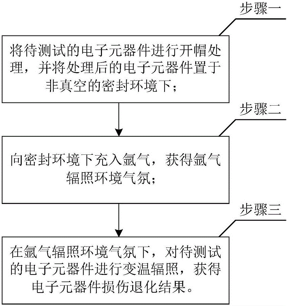
[0030] Specific embodiment 1. The in-situ test method for the high-energy electron irradiation effect of electronic components and parts under the condition of changing temperature based on the argon environment, comprising the following steps:

[0031] Step 1: First place the temperature control device in the sealed chamber, and connect the lead wire of the temperature control device with the vacuum plug of the sealed chamber, and then adjust the temperature range to the required range, namely: 20°C to 500°C;

[0032] Step 2: Uncap the electronic components to be irradiated (that is, the test sample), test the initial parameters once, and then fix the sample on a special fixture and fix it on the temperature control device;

[0033] Step 3: Connect the lead wire of the electrical performance test of the sample to the semiconductor electrical performance tester through the vacuum plug, perform the second initial parameter, and compare it with the result of the previous initial ...

specific Embodiment 2

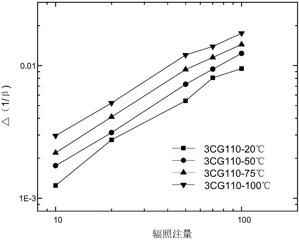
[0036] Specific embodiment two, the in-situ test method of the transistor 3CG110 high-energy electron irradiation effect under the condition of changing the temperature based on the argon environment described in this embodiment, the specific steps of the method are:

[0037] Step 1: First, test the raw data of the bipolar transistor 3CG110, select samples that meet the performance indicators for future use, and record the initial value;

[0038] Step 2: Fix the sealed chamber at the corresponding position of the high-energy electron radiation source, and place a temperature control device in the irradiation area of ​​the sealed chamber, and adjust the temperature of the heating stage until the horizontal plane is perpendicular to the incident direction of electrons;

[0039] Step 3: Uncap the transistor 3CG110 of the sample to be irradiated, test the parameters of 3CG110 with a semiconductor electrical performance tester, and then fix the sample on a special fixture and fix it...


PUM


Abstract

The invention discloses a method for an in-situ test of a high-energy electron irradiation effect of an electronic component under a temperature changing condition based on an argon environment, and relates to the field of electronic technologies. The invention aims to solve the problem that during ground irradiation of an electronic component, due to influence of an environmental atmosphere and a temperature, an electrical property in-situ test is not accurate and the evaluating efficiency is low. The method disclosed by the invention adopts the argon environment, so that the influence of oxygen in the air and the influence of a negative pressure in vacuum irradiation in a process of irradiation test in the past can be effectively eliminated, and the accuracy of the in-situ test of the electronic component can be improved. Temperature-changing irradiation is performed during irradiation, and an environmental temperature condition for work of a bipolar transistor is selected in a temperature interval, so that according to the method, a low-dose rate enhancement effect acceleration test method that the in-situ test method has simple steps and is easy to operate. The method disclosed by the invention is suitable for space irradiation effect research and test of a bipolar electronic component.

Description

technical field [0001] The invention belongs to the field of electronic technology. Background technique [0002] In the ionizing radiation environment, the radiation damage of electronic components under the irradiation of high-energy electrons is difficult to achieve in situ testing of high-energy electrons in vacuum, and even in a vacuum environment, the electronic components are damaged due to the negative pressure after the cap is opened. The influence affects the atmosphere inside the transistor, especially the change of hydrogen. Studies have shown that the performance degradation of electronic components caused by irradiation, especially bipolar transistors, mainly depends on the total number of holes and the number of holes that have not recombined with electrons, and the content of hydrogen will directly affect the number of holes . When holes migrate in the bipolar transistor oxide layer, these holes can react with hydrogen-containing defects to release H + . ...

Claims


Application Information

Patent Timeline
IPC IPC(8): G01R31/00
CPCG01R31/002
Inventor 李兴冀马国亮杨剑群刘超铭
Owner HARBIN INST OF TECH
Why Eureka
Try Eureka