High-voltage power device with special voltage withstanding ring

A high-voltage power device and voltage-resistant ring technology, applied in semiconductor devices, electrical components, circuits, etc., can solve the problems of poor voltage-resistant performance, large area occupied by terminals, and high cost, and achieve cost reduction, chip area reduction, The effect of reducing the area

Pending Publication Date: 2017-01-25
ZHANGJIAGANG EVER POWER SEMICON
View PDF7 Cites 1 Cited by
  • Summary
  • Abstract
  • Description
  • Claims
  • Application Information

AI Technical Summary

Problems solved by technology

Although the invention uses a super junction structure to improve the withstand voltage, its terminal area is p

Method used


Image

  • High-voltage power device with special voltage withstanding ring
  • High-voltage power device with special voltage withstanding ring
  • High-voltage power device with special voltage withstanding ring

Examples


Embodiment Construction

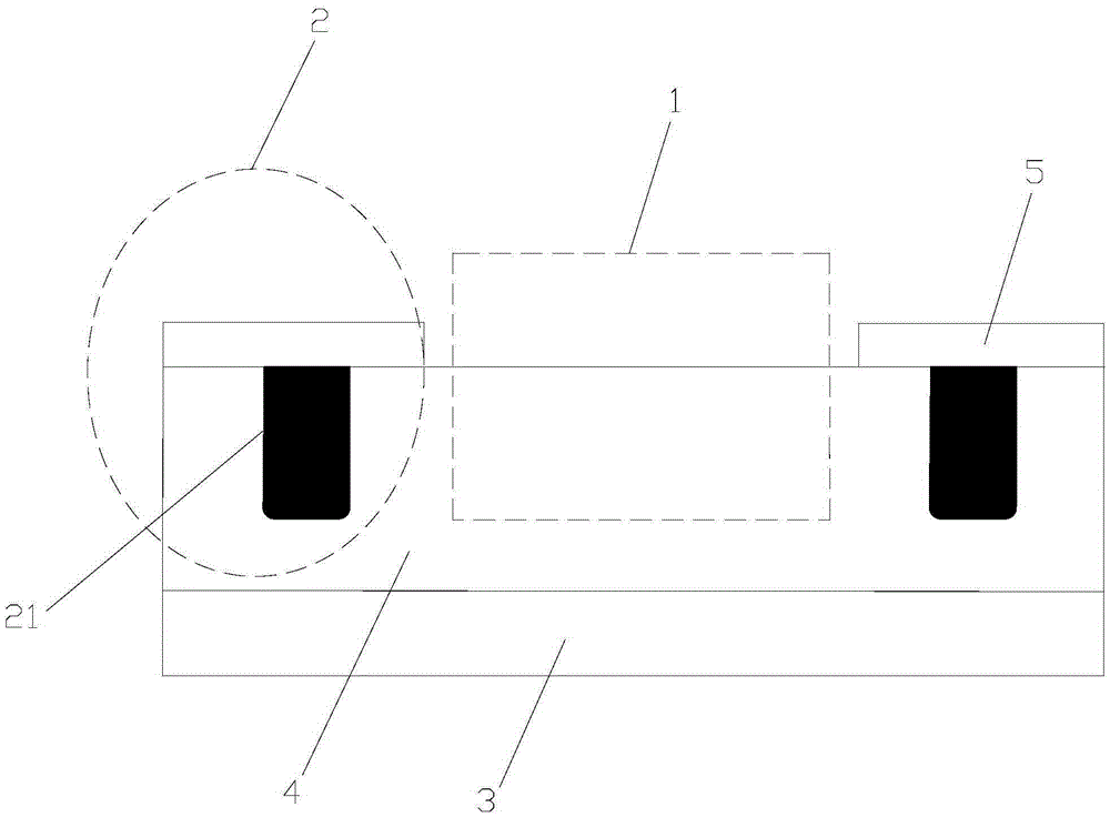
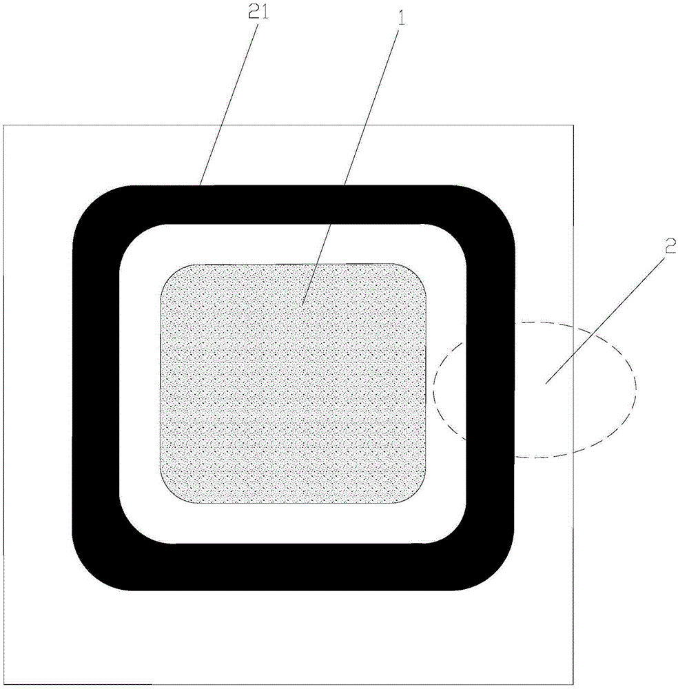
[0022] Such as figure 1 , 2 As shown, the high-voltage power device with a special withstand voltage ring in the present invention can be IGBT, MOSFET, FRD and other devices, including a working area 1 and a terminal area 2 .

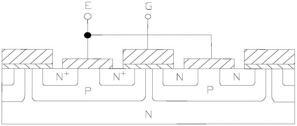
[0023] The working area 1 is located in the middle area of ​​the power device, and the area around the working area 1 is the terminal area 2; where, taking the power device IGBT as an example, image 3 It is the working area 1 of the IGBT, including the gate area G and the emitter area E.

[0024] The substrate 3 of the working region 1 and the terminal region 2 is a heavily doped N+ silicon substrate structure, and the epitaxial layer 4 of the working region 1 and the terminal region 2 is a lightly doped N- epitaxial layer structure and is located on a heavily doped N+ The upper surface of the substrate 3; the thickness of the epitaxial layer 4 is 50-150um.

[0025] The terminal region 2 is provided with a pressure-resistant ring groove 21 downward...


PUM


Abstract

The invention relates to a high-voltage power device with a special voltage withstanding ring. The high-voltage power device comprises a working area (1) and a terminal area (2). The upper surface of a substrate (3) of the working area (1) and the terminal area (2) is provided with an epitaxial layer (4), and the terminal area (2) is provided with a voltage withstanding ring groove (21) downwardly from the upper surface of the epitaxial layer (4). The depth of the voltage withstanding ring groove (21) is smaller than the thickness of the epitaxial layer (4) and internally filled with a light doped P-type GaN material, and the upper surface of the P-type GaN material is flush with the upper surface of the epitaxial layer (4) after filling. Further, the upper surface of the P-type GaN material filled in the voltage withstanding ring groove (21) is covered with an edge passivation layer (5). The high-voltage power device is simple and reasonable in structural design and stable and reliable in use, the area of the terminal area can be effectively reduced while breakdown voltage of the device is effectively boosted, and cost reduction is realized.

Description

technical field [0001] The invention relates to the technical field of semiconductor devices, in particular to a high-voltage power device with a special withstand voltage ring. Background technique [0002] With the rapid development of power electronics technology, high-voltage power devices are also developing in the direction of large capacity, high frequency, high efficiency and energy saving, and low cost. Improving the breakdown voltage of devices has become one of the research directions of people. The ideal device breakdown voltage refers to the case where the pn junction or metal-semiconductor junction is a parallel planar junction. However, due to the influence of certain factors in the actual device and the production process, impurities also undergo lateral diffusion while undergoing vertical diffusion. Diffusion, so the terminal profile of the junction is curved. For high-voltage power devices, when a reverse bias voltage is applied to the junction, the field...

Claims


Application Information

Patent Timeline
IPC IPC(8): H01L29/06H01L29/739
CPCH01L29/0619H01L29/7393
Inventor 周炳石英学郝建勇张志娟
Owner ZHANGJIAGANG EVER POWER SEMICON
Why Eureka
Try Eureka