
Multi-mode waveguide 90-degree turning array chip

An array chip and waveguide technology, applied in the field of multimode waveguide 90° steering array chips, can solve the problems that hinder the miniaturization of active optical cables, low cost of integration, high reliability, high cost of mold opening, optical aging, etc., and achieve Conducive to optical integration, reduce joining and mounting procedures, and good stability

Inactive Publication Date: 2017-02-01
HENAN SHIJIA PHOTONS TECH
View PDF4 Cites 4 Cited by
  • Summary
  • Abstract
  • Description
  • Claims
  • Application Information

AI Technical Summary

Problems solved by technology

However, this Lens array solution has some problems in terms of optical path and structure: First, the optical path is long. The current array lens / 45° reflective surface structure design is to cover the chip (VCSEL and Driver, PIN and TIA) under it. In consideration of the high-speed characteristics, VCSEL and Driver, PIN and TIA must be very close, and a wire bonder is used to connect them with gold wires. Gold wires generally have a wire arc height greater than 100 μm, making the lens There is already a distance of at least 100 μm between the emitting / receiving surface, plus the optical path of the 45° reflective surface and the optical path generated by the connection mechanism with the optical fiber, the light must pass through a path of 400 μm (entering the optical fiber from the VCSEL or passing through the optical fiber) Fiber to PIN), in this case, a small deviation during or after packaging will produce a large offset; second, because the array lens / 45°reflective surface is made by injection molding, in There must be thick structural support around the array lens / 45° reflective surface to prevent deformation during demoulding, so the current array lens / 45° reflective surface has very thick outer walls, making it too bulky; third, the sub-components Many, the design is complicated; fourth, the mold opening precision of the Lens array is very high, and needs to reach the um level, which leads to high mold opening costs and high prices; fifth, the plastic parts in the Lens array will be affected by the laser Optical aging occurs, so it is difficult to apply in scenes with high environmental requirements, such as -40~+85℃
These problems in the Lens array solution hinder the development of active optical cables in terms of miniaturization, integration, low cost, and high reliability.

Method used


Image

  • Multi-mode waveguide 90-degree turning array chip
  • Multi-mode waveguide 90-degree turning array chip
  • Multi-mode waveguide 90-degree turning array chip

Examples


Embodiment Construction

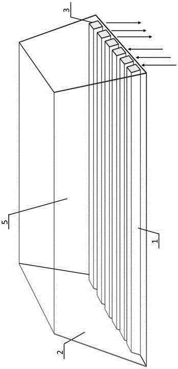
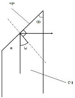
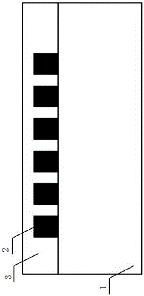
[0022] Such as Figure 1-3 As shown, a multimode waveguide 90° steering array chip includes a chip body 5 , the chip body 5 includes a substrate 1 , a waveguide 2 and a cladding 3 , and the cladding 3 wraps the waveguide 2 on the substrate 1 . The material of the substrate 1 is pure quartz glass. The material of the waveguide 2 is silicon dioxide doped with Ge. The cladding layer 3 is made of silicon dioxide doped with B and P. The cross section of the waveguide can be adjusted according to the specific situation. The thickness of the cladding layer 3 is 15 μm, and the upper and lower ranges can be adjusted.

[0023] The waveguides 2 are arranged in parallel and the intervals between the waveguides 2 are equal. The number of the waveguides and the distance between the waveguides can be adjusted according to specific conditions.

[0024] And one end surface of the waveguide 2 is a total reflection surface 4 . The inclination angle of the total reflection surface 4 is θ, an...


PUM


Abstract

The invention discloses a multi-mode waveguide 90-degree turning array chip comprising a chip body including a substrate, waveguides, and a coating layer. The coating layer enables the waveguides to coat the substrate; the waveguides are parallel to each other and are arranged at equal intervals; and the end surface of one side of each waveguide is a totally reflection surface. The number of the waveguides and the waveguide interval can be adjusted according to specific situations. No lens is introduced; the optical path is short; and light integration can be realized well. Because of direct coupling, the adding and pasting procedures of the lens array are reduced, the coupling precision is high. And the overall stability of the optical path is high. The processing technology of the waveguide array is mature and the cost is low. No expensive lens design and high mode opening cost are needed; and the early-stage research and development investment is reduced. The optical waveguide array is made of a quartz glass material, so that an aging problem at a high temperature is avoided; and reliability on the high or low temperature condition is higher.

Description

[0001] Multimode waveguide 90° steering array chip. technical field [0002] The invention belongs to the field of optical fiber communication, and in particular relates to a multimode waveguide 90° steering array chip. Background technique [0003] In the active optical cable, the integrally formed Lens array including the array lens and the 45° reflective surface is mainly used to realize the 90° conversion of the optical path. However, this Lens array solution has some problems in terms of optical path and structure: First, the optical path is long. The current array lens / 45° reflective surface structure design is to cover the chip (VCSEL and Driver, PIN and TIA) under it. In consideration of the high-speed characteristics, VCSEL and Driver, PIN and TIA must be very close, and a wire bonder is used to connect them with gold wires. Gold wires generally have a wire arc height greater than 100 μm, making the lens There is already a distance of at least 100 μm between the em...

Claims


Application Information

Patent Timeline
IPC IPC(8): G02B6/122
CPCG02B6/122G02B2006/12038G02B2006/12197
Inventor 尹小杰孙静雯刘耀张家顺安俊明钟飞常夏森
Owner HENAN SHIJIA PHOTONS TECH
Learn More