Photoelectric conversion module for realizing optical power monitoring and manufacturing method thereof

A photoelectric conversion module, optical power monitoring technology, applied in the coupling of optical waveguides, electrical components, electromagnetic transmitters, etc., can solve the problems of reducing the reliability of the optical path, many optical path components and optical surfaces, and long optical path, etc. Optical path reliability, ensuring performance stability, and increasing the effect of heat dissipation area

Inactive Publication Date: 2018-01-05
HISENSE & JONHON OPTICAL ELECTRICAL TECH CO LTD
View PDF6 Cites 0 Cited by
  • Summary
  • Abstract
  • Description
  • Claims
  • Application Information

AI Technical Summary

Problems solved by technology

[0003] At present, the monitoring of the life of the optical chip is realized by monitoring the luminous power of the optical chip. In the prior art, the beam is shaped by designing multiple sets of lenses, and the light is realized based on total reflection and beam splitting. Power monitoring and optical transmission, but in the existing implementation, more optical path components and optical surfaces are required, and the optical path is longer, which reduces the reliability of the optical path

Method used


Image

  • Photoelectric conversion module for realizing optical power monitoring and manufacturing method thereof
  • Photoelectric conversion module for realizing optical power monitoring and manufacturing method thereof
  • Photoelectric conversion module for realizing optical power monitoring and manufacturing method thereof

Examples


Embodiment Construction

[0025] The specific implementation manners of the present application will be described in further detail below in conjunction with the accompanying drawings.

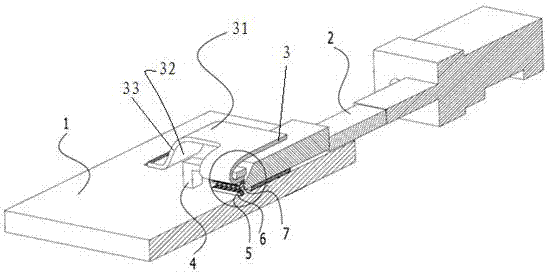
[0026] Such as figure 1 As shown, the photoelectric conversion module proposed by this application to realize optical power monitoring, especially the parallel photoelectric conversion module, includes PCB board 1, optical fiber array assembly 2, flexible board 3, metal bracket 4, laser 5 and detector 7; laser 5 Mount on PCB board 1.

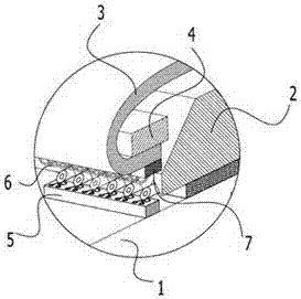
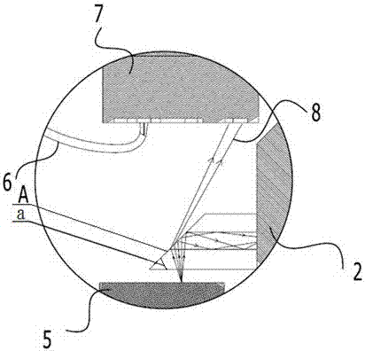
[0027] Specifically, such as figure 2 As shown, the detector 7 is mounted on the first surface 31 of the flexible board 3; the part corresponding to the detector 7 on the second surface 32 of the flexible board 3 opposite to the first surface 31 is connected to the lower end surface of the metal bracket 4; The bracket 4 is welded on the PCB board 1, and the detector 7 is placed relative to the laser 5; as image 3 As shown, the end face A of each fiber of the fiber array assembly 2 i...


PUM


Abstract

The invention discloses a photoelectric conversion module for realizing optical power monitoring and a manufacturing method thereof. The photoelectric conversion module comprises a PCB, an optical fiber array component, a laser, a detector, a flexible board and a metal bracket. The detector is mounted to a first surface of the flexible board. A part corresponding to the detector on a second surface opposite to the first surface of the flexible board is connected to a lower end face of a metal bracket. The metal bracket is welded to the PCB such that the detector is placed to face laser. The end face of each optical fiber of the optical fiber array component has an angle with a set degree relative to the detector or the laser such that a part of laser is refracted to a detection surface ofthe detector and a part of laser is subjected to full reflection to be transmitted through the fiber array component after the laser emitted by the laser is emitted to the end face, and the light emitting power monitoring and optical transmission of the photoelectric conversion module are realized with fewest optical components, a smallest optical surface and a smallest optical distance, and the reliability of an optical path is improved.

Description

technical field [0001] The invention belongs to the technical field of optical fiber communication, and in particular relates to a photoelectric conversion module for realizing optical power monitoring and a manufacturing method thereof. Background technique [0002] With the promotion and application of optical communication products, the demand for parallel photoelectric conversion modules is increasing day by day, and the market demand is also developing in the direction of continuous miniaturization, high speed, high density and high power. Among various optical module products , The monitoring of the life of the optical chip can enable customers to know the performance of the product in time. [0003] At present, the monitoring of the life of the optical chip is realized by monitoring the luminous power of the optical chip. In the prior art, the beam is shaped by designing multiple sets of lenses, and the light is realized based on total reflection and beam splitting. ...

Claims


Application Information

Patent Timeline
Patent Type & Authority Applications(China)
IPC IPC(8): G02B6/42H04B10/079H04B10/50
Inventor 王永乐姜瑜斐仲兆良
Owner HISENSE & JONHON OPTICAL ELECTRICAL TECH CO LTD
Why Eureka
Try Eureka