Electronic product

A technology for electronic products and circuit boards, which is used in electrical digital data processing, instruments, digital data processing components, etc. to achieve good fingerprint imaging effects, improve reliability, and improve assembly structure.

Active Publication Date: 2017-02-08
SHANGHAI OXI TECH
View PDF6 Cites 12 Cited by
  • Summary
  • Abstract
  • Description
  • Claims
  • Application Information

AI Technical Summary

Problems solved by technology

[0004] However, when the existing electronic products are assembled with optical fingerprint

Method used


Image

  • Electronic product
  • Electronic product
  • Electronic product

Examples


Embodiment Construction

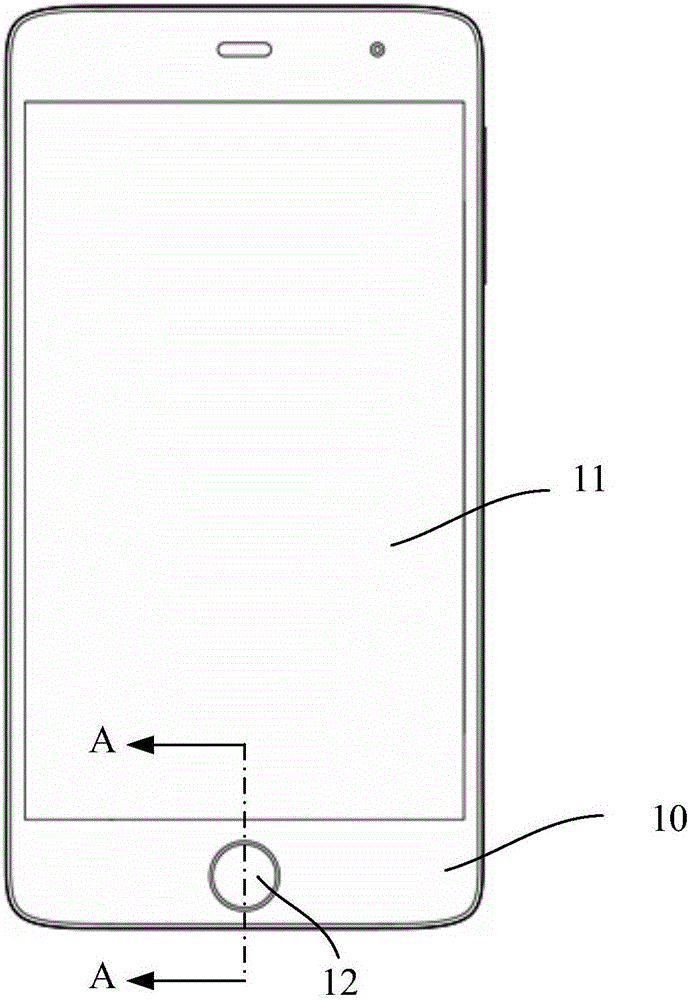
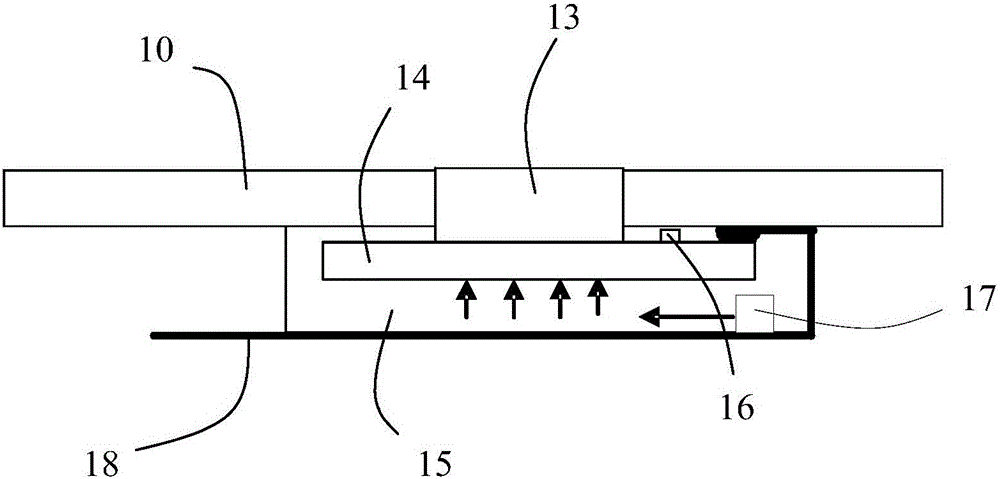
[0038] Please refer to figure 1 with figure 2 , figure 1 Shows a front view of an existing mobile terminal, figure 2 show figure 1 The schematic diagram of the cross-sectional structure of the mobile terminal is cut along the dotted line A-A. The mobile terminal includes an outer cover 10 and a screen 11, and the mobile terminal also includes an optical fingerprint sensor 12. The optical fingerprint sensor 12 happens to be assembled in a through hole on the surface of the outer cover 10 (the through hole is not shown separately, please refer to figure 2 ). figure 2 In the middle display mobile terminal, the optical fingerprint sensor includes a protective cover 13, a pixel substrate 14, and a light guide plate 15 from top to bottom, and the optical fingerprint sensor also includes a signal readout chip 16 on the upper surface of the pixel substrate 14. The light source 17 located in the light guide plate 15 and the flexible printed circuit board 18. The light source 17 is g...


PUM

PropertyMeasurementUnit
Thicknessaaaaaaaaaa

Abstract

An electronic product comprises the following units: an optics fingerprint sensor including a pixel substrate, a light guide plate and a flexible print circuit board, wherein the pixel substrate has a pixel array; an outer cover plate having an outer surface and an inner surface, wherein the outer surface is provided with a first blind hole, and the first blind hole is opposite to the top surface of the pixel array. The pixel substrate comprises a flexible base plate, and comprises a fixed portion and a bending portion, wherein the fixed portion is arranged on the top surface of the light guide plate, and the bending portion is arranged outside the side edge of the light guide plate; the bending portion is bound with the first portion of the flexible print circuit board, and bends downward until the first portion of the flexible print circuit board and the inner surface of the outer cover plate mutually separate from each other or make zero-acting force contacts; the assemble structure of the optics fingerprint sensor in the electronic product is improved, so the assembling difficulty is reduced, thus lowered cost.

Description

Technical field [0001] The invention relates to the field of optical fingerprint identification, and in particular to an electronic product. Background technique [0002] Fingerprint imaging recognition technology is a technology that collects the fingerprint image of the human body through the fingerprint sensor, and then compares it with the existing fingerprint imaging information in the system to determine whether it is correct or not, and then realize the identity recognition technology. Because of its ease of use and the uniqueness of human fingerprints, fingerprint identification technology has been widely used in various fields. For example, security inspection areas such as the Public Security Bureau and customs, building access control systems, and consumer goods areas such as personal computers and mobile phones, etc. The realization of fingerprint imaging technology includes optical imaging, capacitance imaging, ultrasonic imaging and other technologies. Relatively ...

Claims


Application Information

Patent Timeline
IPC IPC(8): G06F1/16
Inventor 凌严朱虹
Owner SHANGHAI OXI TECH
Why Eureka
Try Eureka