Method for realizing all-optical diode

A technology of all-optical diode and realization method, which is applied in the realization field of all-optical diode, can solve the problem of high requirements on the preparation process, and achieve the effect of great application value

Inactive Publication Date: 2017-02-15
NANCHANG HANGKONG UNIVERSITY
View PDF5 Cites 12 Cited by
  • Summary
  • Abstract
  • Description
  • Claims
  • Application Information

AI Technical Summary

Problems solved by technology

However, there are still the following disadvantages: the structure adopts the asymmetric structure design of the photonic crystal waveguide FP cavity and the nonlinear microcavity beside the waveguide. In the photonic crystal waveguide structure, the FP cavity and the microcavity structure must be realized at the same time. relatively high

Method used


Image

  • Method for realizing all-optical diode
  • Method for realizing all-optical diode
  • Method for realizing all-optical diode

Examples


Embodiment

[0017] Embodiment: a preferred implementation case of the present invention is introduced below:

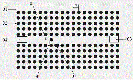
[0018] figure 1 It is a schematic diagram of the structure of an all-optical diode based on a photonic crystal waveguide. The microcavity (Fano) 07 below the line defect waveguide structure introduces an elliptical dielectric column to replace the original circular dielectric column structure, and adds a reflective layer dielectric column 06 in the photonic crystal waveguide near the high-Q nonlinear microcavity, In addition, the resonance peak corresponding to the Fano microcavity 07 is changed from a reflection type to a transmission type, forming a transmission type Fano resonance cavity. And the position of this reflective layer deviates slightly to the left from a lattice position directly above the microcavity, thus breaking the mirror symmetry of the Fano cavity, enabling the asymmetric coupling between the Fano microcavity 07 and the two sides of the photonic crystal wa...


PUM

PropertyMeasurementUnit
optical propertiesaaaaaaaaaa

Abstract

The invention discloses a method for realizing an all-optical diode. In a two-dimensional photonic crystal waveguide, a micro-cavity is designed on the side; and a dielectric column primitive cell is additionally arranged as a reflective layer in the photonic crystal waveguide near the micro-cavity, and the position of the reflective layer is a lattice constant deviated from the position where the waveguide is over against the micro-cavity. When the incident light intensity increases all along, the forward incident light first reaches a power threshold for exciting the nonlinear Kerr effect of the micro-cavity material, and the backward incident light is in a cut-off state under the light intensity, so as to realize the forward conduction/backward cut-off function of the all-optical diode. The working band of the all-optical diode can be adjusted by adjusting the lattice constant, and the all-optical diode is easy to be integrated in an all-optical network, so that the all-optical diode has a great application value. The all-optical diode has a response time on the order of picosecond, and the photonic crystal has the characteristic of adjusting the forbidden band range according to the lattice constant of the photonic crystal.

Description

technical field [0001] The invention relates to a method for realizing an all-optical diode by using a nonlinear photonic crystal, in particular to a method for realizing an all-optical diode by using an asymmetric coupling structure of a two-dimensional photonic crystal waveguide and a microcavity. Background technique [0002] Today, with the increasing amount of information, the traditional information network can no longer meet people's needs. The emergence of new material photonic crystals has become inevitable. more space [0003] As one of the key components of all-optical signal processing in the future, the all-optical diode must continuously study its implementation method, improve and perfect it to make it more convenient and efficient to realize the functions of forward conduction and reverse cut-off. The dual-cavity all-optical diode designed in the present invention does not need external energy to stimulate pumping, and it is completely all-optical control be...

Claims


Application Information

Patent Timeline
Patent Type & Authority Applications(China)
IPC IPC(8): G02F1/365G02B6/122
CPCG02B6/1225G02F1/365
Inventor 刘彬胡金凤梁红勤刘云凤
Owner NANCHANG HANGKONG UNIVERSITY
Why Eureka
Try Eureka