P type layer open pipe Al diffusion silicon element and preparation method thereof

A technology for diffusing silicon and components, which is applied in the field of P-type layer open-tube Al diffusion silicon components and their preparation, can solve the problems of low surface concentration, poor diffusion consistency, poor intra-chip uniformity, etc., and achieves low equipment requirements and simple preparation method. , The effect of strong industrialization

Inactive Publication Date: 2017-02-22
富芯微电子有限公司
View PDF3 Cites 0 Cited by
  • Summary
  • Abstract
  • Description
  • Claims
  • Application Information

AI Technical Summary

Problems solved by technology

[0004] The technical problem to be solved in the present invention is: vacuum pure Al closed tube diffusion or Al(NO 3 ) 3 Under the two processes of coating diffusion, the surface concentration is low, the uniformity in the chip is poor, and the diffusion consistency is poor

Method used


Image

  • P type layer open pipe Al diffusion silicon element and preparation method thereof
  • P type layer open pipe Al diffusion silicon element and preparation method thereof
  • P type layer open pipe Al diffusion silicon element and preparation method thereof

Examples


Embodiment 1

[0028] A method for preparing a P-type layer open tube Al diffused silicon element, comprising the following steps:

[0029] Step 1, coating an Al film on the Si surface;

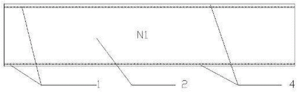
[0030] Step 2, Al-Si alloy layer 1 is formed by alloying, such as figure 1 As shown, that is, the Si surface includes an Al-Si alloy layer 1 and an Al film layer 4;

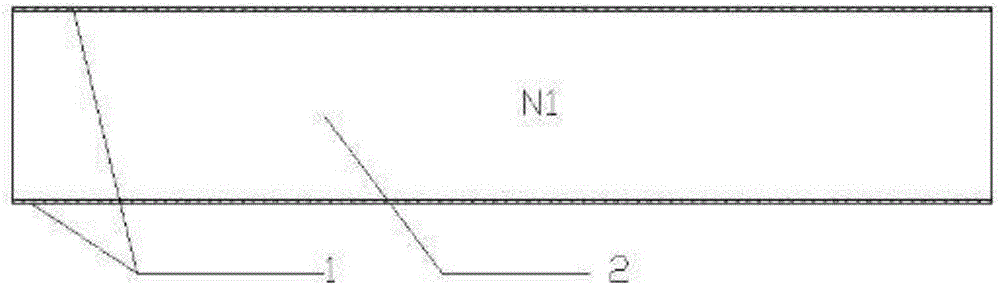
[0031] Step 3, remove the Al film layer 4, such as figure 2 As shown, the Al-Si alloy layer 1 is obtained as the Al impurity source;

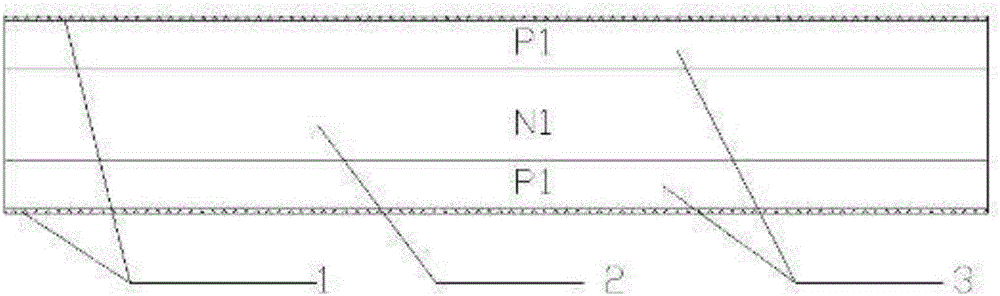
[0032] Step 4: advance the junction depth of the Al-Si alloy layer 1 and the Si layer at a certain temperature and a certain atmosphere for a certain period of time, so that Al diffuses to Si, that is, the formation of image 3 the structure shown;

[0033] Step five, post-processing, that is, to obtain the product.

[0034] Specifically, such as figure 1 As shown, the N-type high-resistance silicon chip used in the high-voltage rectifying element and the high-voltage thyristor constitutes the N-type hig...

Embodiment 2

[0038] A method for preparing a P-type layer open tube Al diffused silicon element, comprising the following steps:

[0039] Step 1, coating an Al film on the Si surface;

[0040] Step 2, forming an Al-Si alloy layer by alloying, such as figure 1 As shown, that is, the Si surface includes an Al-Si alloy layer 1 and an Al film layer 4;

[0041] Step 3, remove the Al film layer 4, such as figure 2 As shown, the Al-Si alloy layer 1 is obtained as the Al impurity source;

[0042] Step 4: advance the junction depth of the Al-Si alloy layer 1 and the Si layer at a certain temperature and a certain atmosphere for a certain period of time, so that Al diffuses to Si, that is, the formation of image 3 the structure shown;

[0043] Step five, post-processing, that is, to obtain the product.

[0044] Specifically, such as figure 1 As shown, the N-type high-resistance silicon wafer used for the high-voltage rectifier element and the high-voltage thyristor constitutes the N-type hig...

Embodiment 3

[0048] A method for preparing a P-type layer open tube Al diffused silicon element, comprising the following steps:

[0049] Step 1, coating an Al film on the Si surface;

[0050]Step 2, forming an Al-Si alloy layer by alloying, such as figure 1 As shown, that is, the Si surface includes an Al-Si alloy layer 1 and an Al film layer 4;

[0051] Step 3, remove the Al film layer 4, such as figure 2 As shown, the Al-Si alloy layer 1 is obtained as the Al impurity source;

[0052] Step 4: advance the junction depth of the Al-Si alloy layer 1 and the Si layer at a certain temperature and a certain atmosphere for a certain period of time, so that Al diffuses to Si, that is, the formation of image 3 the structure shown;

[0053] Step five, post-processing, that is, to obtain the product.

[0054] Specifically, such as figure 1 As shown, the N-type high-resistance silicon wafer used for the high-voltage rectifier element and the high-voltage thyristor constitutes the N-type high...


PUM

PropertyMeasurementUnit
electrical resistivityaaaaaaaaaa

Abstract

The invention relates to the field of thyristors, in particular to a preparation method of a P type layer open pipe Al diffusion silicon element. The preparation method comprises the following steps: firstly, plating an Al film layer on a Si surface; secondly, forming an Al-Si alloy layer in an alloying way, namely the Si surface comprises an Al-Si alloy layer and the Al film layer; thirdly, removing the Al film layer, thus obtaining the Al-Si alloy layer as an Al impurity source; fourthly, advancing junction depth of the Al-Si alloy layer and the Si layer for a certain time at a certain temperature and under certain atmosphere, so that Al diffuses toward Si; and fifthly, carrying out aftertreatment, so that the product is obtained. The preparation method provided by the invention is simple in technology, strong in industrialization capability, low in requirement on equipment, good in product uniformity and good in diffusion consistency.

Description

technical field [0001] The invention relates to the field of thyristor elements, in particular to a P-type layer open tube Al diffused silicon element and a preparation method thereof. Background technique [0002] Thyristor element, short for silicon controlled rectifier element, is a high-power semiconductor device. With the characteristics of small size, relatively simple structure, and strong functions, it is one of the more commonly used semiconductor devices. The device is widely used in various electronic equipment and electronic products, and is mostly used for controllable rectification, inverter, frequency conversion, voltage regulation, non-contact switch, etc. Dimming lamps, speed-adjusting fans, air conditioners, televisions, refrigerators, washing machines, cameras, combined audio systems, sound and light circuits, timing controllers, toy devices, radio remote controls, cameras and industrial controls in household appliances are widely used A thyristor device...

Claims


Application Information

Patent Timeline
Patent Type & Authority Applications(China)
IPC IPC(8): H01L21/228H01L21/332H01L29/74
CPCH01L21/228H01L29/66363H01L29/74
Inventor 陆益刘宗帅纪锦程顾晶伟
Owner 富芯微电子有限公司
Why Eureka
Try Eureka