OLED (organic light-emitting diode) display device and manufacture method thereof

A display device and pixel technology, which is applied in semiconductor/solid-state device manufacturing, semiconductor devices, electrical components, etc., can solve the problems of light-emitting pixels stealing, uneven display, etc., achieve uniform display, reduce light transmittance, and improve product quality. rate effect

Active Publication Date: 2017-02-22
WUHAN TIANMA MICRO ELECTRONICS CO LTD +1
View PDF4 Cites 41 Cited by
  • Summary
  • Abstract
  • Description
  • Claims
  • Application Information

AI Technical Summary

Problems solved by technology

[0007] In view of this, the present invention provides an OLED display device and a manufacturing method thereof, so as to solve the problems of uneven display and light-emitting pixels in the display process of the OLED display device in the prior art.

Method used


Image

  • OLED (organic light-emitting diode) display device and manufacture method thereof
  • OLED (organic light-emitting diode) display device and manufacture method thereof
  • OLED (organic light-emitting diode) display device and manufacture method thereof

Examples


Embodiment Construction

[0036] The following will clearly and completely describe the technical solutions in the embodiments of the present invention with reference to the accompanying drawings in the embodiments of the present invention. Obviously, the described embodiments are only some, not all, embodiments of the present invention. Based on the embodiments of the present invention, all other embodiments obtained by persons of ordinary skill in the art without making creative efforts belong to the protection scope of the present invention.

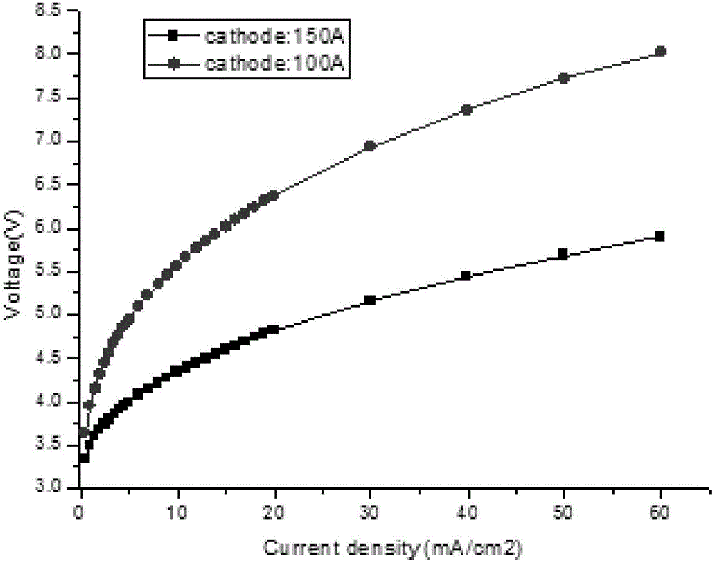
[0037] like figure 2 as shown, figure 2 For OLED display devices with different thickness cathodes under different currents, the corresponding start-up voltage values, figure 2 The middle abscissa is the current density, and the ordinate is the starting voltage. Among them, the small dots represent the thickness of the cathode. OLED display device, the square represents the thickness of the cathode is OLED display device. It can be seen from the dat...


PUM


Abstract

The application discloses an OLED (organic light-emitting diode) display device and a manufacture method thereof; the OLED display device comprises a substrate, an anode layer, a pixel definition layer, a hole injection layer, a hole transport layer, a light-emitting layer, an electronic transport layer, an electronic injection layer, spacer pillars, passivating pillars positioned on the spacer pillars, and a cathode layer, wherein conductive pillars are electrically connected to the cathode layer. By electrically connecting the conductive pillars to the cathode layer, it is equivalent that a conductive resistor is connected parallelly to the cathode layer, resistance of the cathode layer is decreased, voltage drop of the cathode layer is decreased accordingly, and the OLED display device can provide more uniform displaying at the premise of not increasing the thickness of the cathode layer or decreasing the light transmittance of the cathode layer. With the presence of the passivating pillars, lateral leaking current between adjacent light-emitting pixels is decreased, the problem of brightness possessing by pixels is avoided, color mixing rate is deceased, and product yield is increased.

Description

technical field [0001] The present invention relates to the field of display technology, in particular to an OLED (Organic Light Emitting Diode, Organic Light Emitting Diode) display device and a manufacturing method thereof. Background technique [0002] OLED display technology has the characteristics of self-illumination, the following will refer to figure 1 Describe the structure of a typical OLED display device, figure 1 A structural cross-sectional view of a typical OLED display device is schematically shown. [0003] refer to figure 1 , the OLED display device structure mainly includes: a pixel definition layer for defining light-emitting pixels, and the pixel definition layer includes a pixel area and a pixel interval area 02; a spacer column 03 located above the pixel interval area; and a light-emitting pixel; wherein, each Each light emitting pixel includes an anode 01 , a hole injection layer, a hole transport layer, a light emitting layer 05 , an electron trans...

Claims


Application Information

Patent Timeline
Patent Type & Authority Applications(China)
IPC IPC(8): H01L27/32H01L51/56
CPCH10K59/35H10K59/122H10K59/1315H10K71/00
Inventor 刘海民熊志勇
Owner WUHAN TIANMA MICRO ELECTRONICS CO LTD
Why Eureka
Try Eureka