Charge-number mixed accumulation type CMOS-TDI image sensor

An image sensor and accumulative technology, applied in image communication, television, electrical components, etc., can solve the problems of limited accumulative speed and very strict speed requirements, and achieve the effect of reducing speed requirements

Inactive Publication Date: 2017-02-22
TIANJIN UNIV
View PDF4 Cites 7 Cited by
  • Summary
  • Abstract
  • Description
  • Claims
  • Application Information

AI Technical Summary

Problems solved by technology

The third is the digital domain accumulation scheme. In this scheme, the pixel output signal is directly sent to the ADC for quantization, and then the quantized digital quantity is sent to the digital accumulator to realize the accumulation of the signal, but the speed of the ADC is required by this scheme. Very strict, its accumulation rate is limited by the speed of the ADC

Method used


Image

  • Charge-number mixed accumulation type CMOS-TDI image sensor
  • Charge-number mixed accumulation type CMOS-TDI image sensor
  • Charge-number mixed accumulation type CMOS-TDI image sensor

Examples


Embodiment Construction

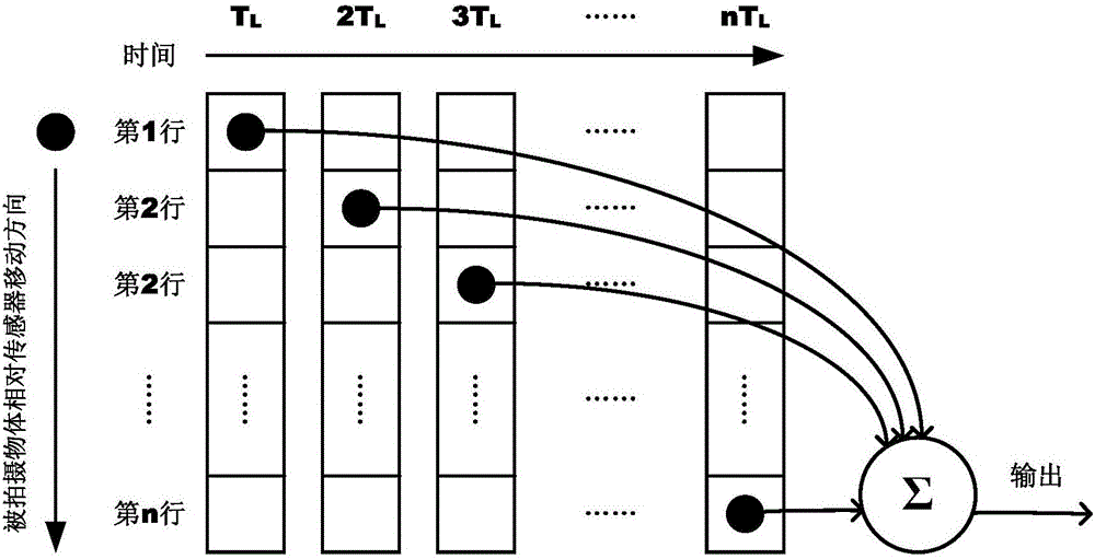
[0014] The analog domain accumulation scheme is to accumulate the voltage signal or current signal obtained by pixel exposure at the output end of the pixel array, and then quantize and output the accumulated signal through the ADC. This solution needs to integrate an analog domain accumulator inside the chip, and usually the analog accumulator is realized through an integral capacitor. Therefore, when the accumulation level is relatively high, the capacitor array will occupy a large chip area, and when the accumulation level is high, the accumulated signal will reach the upper limit, resulting in the loss of image information. The digital domain accumulation scheme is to quantize the signal generated by the pixel exposure through the ADC to generate a binary code value, accumulate the binary code value in the digital accumulator, and finally output the result. Because the accumulator is implemented by a digital circuit, the chip area is small, and the accumulated information ...


PUM


Abstract

The invention relates to the field of analog integrated circuit design. In order to fully exert the advantages that a charge field achieves accumulation without generating noise, and a numeric field accumulation chip is small in area and free of accumulation upper limit and not raise the overhigh requirements on the transmission efficiency and the full well capacity which are generated during charge field accumulation and the ADC speed generated during numeric field accumulation, a charge-number mixed accumulation type CMOS-TDI image sensor characterized by being composed of a pixel array, a column parallel ADC array, a column parallel numeric field accumulation array, a shifting register and a time sequence control module, wherein the pixel array comprises L columns and N rows, N rows of pixels in the pixel array are divided into K pixel subarrays, each pixel subarray is composed of M rows of pixels and a reading circuit, a charge accumulation mode is adopted among all levels of each pixel subarray, a numeric accumulation mode is adopted among the K subarrays, and N, M and K meet the formula N=M*K. The charge-number mixed accumulation type CMOS-TDI image sensor is mainly applied in integrated circuit design.

Description

technical field [0001] The invention relates to the field of analog integrated circuit design, in particular to the field of CMOS-TDI image sensing design. Background technique [0002] Image sensors convert captured images into electrical signals that are easy to store, transmit, and process. For different working environments, image sensors work in different ways, mainly divided into: area array and line array. Among them, the pixel array of the area array image sensor is arranged in a two-dimensional area array, and a complete image can be obtained by only one exposure, which is mainly used in mobile phones and digital cameras. The pixel array of the linear array image sensor is arranged in a one-dimensional linear array, which scans and images relatively moving objects. It is mainly used in medical imaging, industrial inspection, aerospace, etc., and its working method can be referred to figure 1 . Since the scene captured by the line-array image sensor is always movi...

Claims


Application Information

Patent Timeline
Patent Type & Authority Applications(China)
IPC IPC(8): H04N5/374H04N5/3745H04N5/378
CPCH04N25/768H04N25/772H04N25/75
Inventor 高静黄蕊聂凯明徐江涛
Owner TIANJIN UNIV
Why Eureka
Try Eureka