Light Irradiation Type Heat Treatment Method And Heat Treatment Apparatus

A heat treatment method and technology of a heat treatment device, which are applied in the manufacture of electrical components, circuits, semiconductors/solid-state devices, etc., can solve problems such as interface property degradation and high resistance, and achieve the effects of preventing roll-up and improving production capacity

Active Publication Date: 2017-03-08
DAINIPPON SCREEN MTG CO LTD
View PDF9 Cites 3 Cited by
  • Summary
  • Abstract
  • Description
  • Claims
  • Application Information

AI Technical Summary

Problems solved by technology

[0008] However, as shown in Patent Document 1, when the semiconductor wafer on which the metal film is formed is only irradiated with the flash light to perform the flash heat treatment for a very short time, the interface characteristics between the silicide and the silicon in the base layer deteriorate to cause high resistance.

Method used


Image

  • Light Irradiation Type Heat Treatment Method And Heat Treatment Apparatus
  • Light Irradiation Type Heat Treatment Method And Heat Treatment Apparatus
  • Light Irradiation Type Heat Treatment Method And Heat Treatment Apparatus

Examples


no. 1 approach

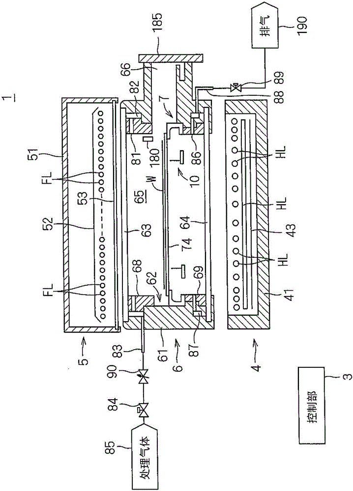
[0119] figure 1 It is a longitudinal sectional view showing the structure of the heat treatment apparatus 1 of the present invention. The heat treatment apparatus 1 of this embodiment is a flash lamp annealing apparatus which heats the semiconductor wafer W by irradiating flash light to the disc-shaped semiconductor wafer W which is a board|substrate. The size of the semiconductor wafer W to be processed is not particularly limited, for example, or A metal film such as nickel is formed on the semiconductor wafer W before being carried into the heat treatment apparatus 1 , and a silicide that is a compound of the metal and silicon is formed and grown by heat treatment in the heat treatment apparatus 1 . In addition, in figure 1 In each of the following figures, the size and quantity of each part are enlarged or simplified as necessary for ease of understanding.

[0120] The thermal processing apparatus 1 has a chamber 6 for accommodating a semiconductor wafer W, a flash h...

no. 2 approach

[0184] Next, a second embodiment of the present invention will be described. The structure of the heat treatment apparatus 1 of the second embodiment is completely the same as that of the first embodiment. In addition, the processing procedure of the semiconductor wafer W in the thermal processing apparatus 1 of the second embodiment is also substantially the same as that of the first embodiment. The second embodiment differs from the first embodiment in that the pressure in the chamber 6 is restored after the pressure in the chamber 6 is decompressed once.

[0185] Figure 11 It is a figure which shows the pressure change in the chamber 6 in 2nd Embodiment. exist Figure 11 in, with Figure 10 Similarly, the horizontal axis represents the time, and the vertical axis represents the pressure in the chamber 6 . in addition, Figure 11 The pattern shown by the dotted line in is the pressure change pattern ( Figure 10 picture of).

[0186] As in the first embodiment, when...

no. 3 approach

[0201] Next, a third embodiment of the present invention will be described. The structure of the heat treatment apparatus 1 of the third embodiment is completely the same as that of the first embodiment. In addition, the processing procedure of the semiconductor wafer W in the thermal processing apparatus 1 of the third embodiment is also substantially the same as that of the first embodiment. The third embodiment differs from the first embodiment in that the pressure inside the chamber 6 changes.

[0202] Figure 12 It is a figure which shows the pressure change in the chamber 6 in 3rd Embodiment. exist Figure 12 in, with Figure 10 Similarly, the horizontal axis represents the time, and the vertical axis represents the pressure in the chamber 6 .

[0203] As in the first embodiment, when the semiconductor wafer W on which the metal film 108 is formed is accommodated in the chamber 6 and the transfer opening 66 is closed, the pressure in the chamber 6 is normal pressure...


PUM


Abstract

A metal film is deposited on a front surface of a semiconductor wafer of silicon. After the semiconductor wafer is received in a chamber, the pressure in the chamber is reduced to a pressure lower than atmospheric pressure. Thereafter, nitrogen gas is supplied into the chamber to return the pressure in the chamber to ordinary pressure, and the front surface of the semiconductor wafer is irradiated with a flash of light, so that a silicide that is a compound of the metal film and silicon is formed. The oxygen concentration in the chamber is significantly lowered during the formation of the silicide because the pressure in the chamber is reduced once to the pressure lower than atmospheric pressure and then returned to the ordinary pressure. This suppresses the increase in resistance of the silicide resulting from the entry of oxygen in the atmosphere in the chamber into defects near the interface between the metal film and a base material.

Description

technical field [0001] The present invention relates to a heat treatment method and a heat treatment apparatus for forming silicide or germanide by irradiating flash light on a silicon or silicon germanium thin-plate precision electronic substrate (hereinafter, simply referred to as "substrate") such as a semiconductor wafer. Background technique [0002] In the manufacturing process of semiconductor devices, flash lamp annealing (FLA), which heats a semiconductor wafer in an extremely short time, is attracting attention. Flash lamp annealing is a heat treatment technique that irradiates a flash of light on the surface of a semiconductor wafer using a xenon flash lamp (hereinafter referred to simply as a "flash lamp" means a xenon flash lamp) so that only the semiconductor wafer The surface of the wafer heats up. [0003] The radiation spectrum of the xenon flash lamp is distributed from the ultraviolet region to the near infrared region, and the wavelength is shorter than ...

Claims


Application Information

Patent Timeline
Patent Type & Authority Applications(China)
IPC IPC(8): H01L21/268H01L21/285H01L21/67
CPCH01L21/2686H01L21/28518H01L21/67115H01L21/268H01L21/265H01L21/67253H01L21/67248H01L21/68707
Inventor 青山敬幸河原崎光古川雅志布施和彦谷村英昭加藤慎一
Owner DAINIPPON SCREEN MTG CO LTD
Why Eureka
Try Eureka