InGaP wet etching method

A wet etching and epitaxial layer technology, applied in electrical components, semiconductor/solid-state device manufacturing, circuits, etc., can solve problems such as the inability to guarantee the smooth progress of the HBT process, and achieve the effect of removing the influence and ensuring the smooth progress.

Active Publication Date: 2017-03-08
CHENGDU HIWAFER SEMICON CO LTD
View PDF4 Cites 4 Cited by
  • Summary
  • Abstract
  • Description
  • Claims
  • Application Information

AI Technical Summary

Problems solved by technology

[0015] The embodiment of the present invention provides an InGaP wet etching method, which solves the problem that the HBT process cannot be guaranteed to proceed smoothly due to the influence of the previous process on the surface of the InGaP layer when etching the InGaP layer in the prior art.

Method used


Image

  • InGaP wet etching method

Examples


Embodiment Construction

[0027] The embodiment of the present invention provides an InGaP wet etching method, which solves the problem that in the prior art, when etching the InGaP layer, the smooth progress of the HBT process cannot be guaranteed due to the influence of the previous process on the surface of the InGaP layer.

[0028] In order to solve the above-mentioned technical problems, the technical solution of the present invention will be described in detail below in conjunction with the accompanying drawings and specific implementation methods.

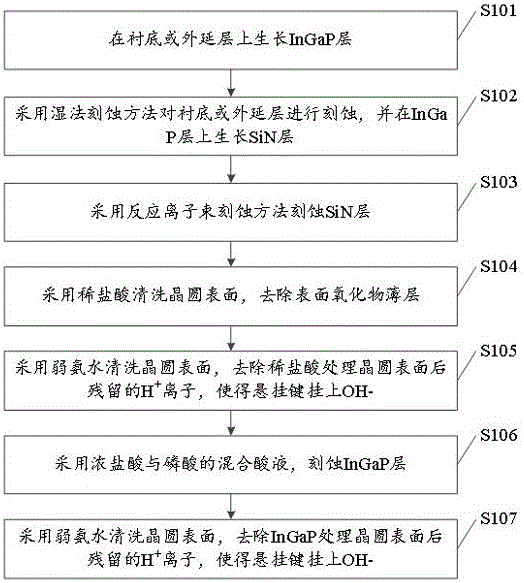
[0029] The invention provides a wet etching method of InGaP, such as figure 1 As shown, it includes: S101, growing an InGaP layer on a substrate or an epitaxial layer, the material of the substrate is any one of GaAs, InP, Si, and SiC, and the epitaxial layer is specifically a GaAs epitaxial layer, an InP epitaxial layer Any one, the thickness of the InGaP layer is 100 Å~1μm.

[0030] Next, in S102, the substrate or the epitaxial layer is etched by ...


PUM


Abstract

The invention relates to the technical field of semiconductor manufacturing, and particularly relates to an InGaP wet etching method. The method comprises the following steps: an InGaP layer grows on a substrate or an epitaxial layer; a wet etching method is adopted to etch the substrate or the epitaxial layer, and an SiN layer grows on the InGaP layer; a reactive ion beam etching method is adopted to etch the SiN layer; dilute hydrochloric acid is adopted to clean the surface of a wafer, and a surface oxide thin layer is removed; weak ammonia is adopted to clean the surface of the wafer, residual H<+> ions after the dilute hydrochloric acid processes the surface of the wafer are removed, and OH- is dangled on a dangling bond; a mixed acid solution of concentrated hydrochloric acid and phosphoric acid is adopted to etch the InGaP layer; and the weak ammonia is adopted to clean the surface of the wafer, residual H<+> ions after the wafer surface is processed by InGaP, and OH- is dangled on a dangling bond. Influences on the surface of the InGaP layer by a preceding process can be removed, and smooth going of the HBT process is ensured.

Description

technical field [0001] The invention relates to the technical field of semiconductor manufacturing, in particular to an InGaP wet etching method. Background technique [0002] GaAs is the most important and widely used semiconductor material among III-V compound semiconductors. The electron mobility in GaAs is 6 times that of silicon (Si), and its electron peak drift velocity is 2 times that of Si. Therefore, GaAs devices have the characteristics of high frequency, high speed, low power consumption, low noise, and monolithic integration. [0003] GaAs HBT devices are widely used in smartphones and base stations, which have the following advantages (source doctoral thesis: Research on InGaP / GaAs microwave HBT devices and VCO circuits): [0004] 1. Single positive power supply operation. Unlike depletion-type FET and HEMT devices, a negative voltage must be applied to pinch off the channel. The turn-on voltages of HBT are all positive, and only one positive power supply is...

Claims


Application Information

Patent Timeline
Patent Type & Authority Applications(China)
IPC IPC(8): H01L21/306H01L21/02
CPCH01L21/02057H01L21/30612
Inventor 陈一峰
Owner CHENGDU HIWAFER SEMICON CO LTD
Why Eureka
Try Eureka