
LED epitaxial structure with high hole injection efficiency

A technology of injection efficiency and epitaxial structure, applied in the direction of electrical components, circuits, semiconductor devices, etc., can solve the problem of low hole concentration, achieve the effect of increasing hole concentration, improving hole mobility, and reducing electron overflow

Inactive Publication Date: 2017-03-08
NANTONG TONGFANG SEMICON +1
View PDF5 Cites 8 Cited by
  • Summary
  • Abstract
  • Description
  • Claims
  • Application Information

AI Technical Summary

Problems solved by technology

However, since the activation energy of Mg in AlGaN is as high as 150-250meV, the hole concentration at room temperature is very low, and only a small amount of Mg can be activated.

Method used


Image

  • LED epitaxial structure with high hole injection efficiency

Examples


Embodiment 1

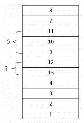
[0017] (1) The sapphire substrate 1 is subjected to a high-temperature cleaning treatment at 1000° C. for 10 minutes, and then a nitriding treatment is performed.

[0018] (2) Lower the temperature to 500° C., grow a GaN buffer layer 2 with a thickness of 100 angstroms and a pressure of 300 Torr.

[0019] (3) Without trimethylgallium (TMGa), raise the temperature to 1000°C, anneal the GaN buffer layer 2 for 3 minutes, and then pass through TMGa to grow the undoped GaN layer 3 with a thickness of 1 μm, pressure It is 300 Torr.

[0020] (4) Disilane is introduced at a temperature of 1000° C. to grow an N-type GaN layer 4 with a thickness of 2 μm and a pressure of 100 Torr.

[0021] (5) After the growth of the N-type GaN layer 4 is completed, the multi-quantum well 5 is grown, and the multi-quantum well 5 is composed of the InGaN layer 13 and the GaN layer 12 . The growth temperature of the GaN layer 12 is 800°C and the thickness is 100 angstroms, the growth temperature of the ...

Embodiment 2

[0027] (1) The sapphire substrate 1 is subjected to a high-temperature cleaning treatment at 1100° C. for 20 minutes, and then a nitriding treatment is performed.

[0028] (2) Lower the temperature to 600° C., grow a GaN buffer layer 2 with a thickness of 200 angstroms and a pressure of 450 Torr.

[0029] (3) Without trimethylgallium (TMGa), the temperature was raised to 1100°C, and the GaN buffer layer 2 was annealed for 4 minutes, and then TMGa was injected to grow the undoped GaN layer 3 with a thickness of 1.5 μm. The pressure is 400 Torr.

[0030] (4) Disilane is introduced at a temperature of 1100° C. to grow an N-type GaN layer 4 with a thickness of 3 μm and a pressure of 200 Torr.

[0031] (5) After the growth of the N-type GaN layer 4 is completed, the multi-quantum well 5 is grown, and the multi-quantum well 5 is composed of the InGaN layer 13 and the GaN layer 12 . The growth temperature of the GaN layer 12 is 850°C and the thickness is 110 angstroms, the growth t...

Embodiment 3

[0037] (1) The sapphire substrate 1 is subjected to a high-temperature cleaning treatment at 1200° C. for 30 minutes, and then to a nitriding treatment.

[0038] (2) Lower the temperature to 700° C., grow a GaN buffer layer 2 with a thickness of 300 angstroms and a pressure of 600 Torr.

[0039] (3) Without trimethylgallium (TMGa), raise the temperature to 1200°C, anneal the GaN buffer layer 2 for 5 minutes, and then pass through TMGa to grow the undoped GaN layer 3 with a thickness of 2 μm and pressure It is 500 Torr.

[0040] (4) Disilane is injected at a temperature of 1200° C. to grow an N-type GaN layer 4 with a thickness of 4 μm and a pressure of 300 Torr.

[0041] (5) After the growth of the N-type GaN layer 4 is completed, the multi-quantum well 5 is grown, and the multi-quantum well 5 is composed of the InGaN layer 13 and the GaN layer 12 . The growth temperature of the GaN layer 12 is 900°C and the thickness is 120 angstroms; the growth temperature of the InGaN lay...


PUM

PropertyMeasurementUnit
Thicknessaaaaaaaaaa

Abstract

The invention discloses an LED epitaxial structure with high hole injection efficiency, and relates to the technical field of light emitting diode epitaxy. The LED epitaxial structure sequentially comprises a substrate, a GaN buffer layer, a non-doped GaN layer, an N-type GaN layer, a multiple-quantum well, an electron blocking layer, a P-type GaN layer and a P-type contact layer from bottom to top, wherein the multiple-quantum well comprises an InGaN layer and a GaN layer, the structure of the LED epitaxial structure is characterized in that the electron blocking layer sequentially comprises a p-type Al<x>Ga<1-x>N layer, an AlN layer and a p-type In<y>Ga<1-y>N layer from bottom to top, x is more than 0 but less than or equal to 0.3, y is more than 0 but less than or equal to 0.2, the electronic blocking layer comprises 8-12 growth periods, the growth pressure is 100-200Torr, and the electronic blocking layer is grown in a nitrogen environment. The electron blocking layer comprises the p-type Al<x>Ga<1-x>N layer, the AlN layer and the p-type In<y>Ga<1-y>N superlattice layer, hole concentration and mobility are improved by stress and by reducing alloy scattering, and the luminous efficiency of a light emitting diode is improved.

Description

technical field [0001] The invention relates to the technical field of light-emitting diode epitaxy, in particular to an LED epitaxy structure with high hole injection efficiency. Background technique [0002] III-V nitride light-emitting diodes have the advantages of high efficiency, energy saving, environmental protection, and long life, and have important applications in the field of solid-state lighting. As the application range of III-V nitride light-emitting diodes increases, the requirements for the photoelectric characteristics of light-emitting diodes are also getting higher and higher. [0003] In the prior art, due to the phenomenon of efficiency drop (Efficiency Droop) caused by polarization effect and electron overflow, p-type AlGaN is commonly used as an electron blocking layer to reduce electron overflow and improve brightness. However, since the activation energy of Mg in AlGaN is as high as 150-250meV, the hole concentration at room temperature is very low,...

Claims


Application Information

Patent Timeline
IPC IPC(8): H01L33/14H01L33/06H01L33/00
CPCH01L33/145H01L33/0066H01L33/0075H01L33/06
Inventor 郑建钦田宇吴真龙曾颀尧赖志豪林政志
Owner NANTONG TONGFANG SEMICON
Learn More