Anti-ferroelectric-paraelectric material coupled capacitor dielectric and preparation method therefor

An antiferroelectric and capacitor technology, applied in the field of capacitors, can solve problems such as voltage resistance and energy storage efficiency bottlenecks, and achieve the effect of large energy storage density

Inactive Publication Date: 2017-03-22
SOUTH CHINA NORMAL UNIVERSITY
View PDF8 Cites 2 Cited by
  • Summary
  • Abstract
  • Description
  • Claims
  • Application Information

AI Technical Summary

Problems solved by technology

[0003] Research on new capacitor materials emerges in an endless stream, mainly including research on ceramics and thick films doped with lead zirconate titanate series elements, research on organic ferroelectric materials polyvinylidene fluoride PVDF and its copolymers, and research on multivariate relaxor ferroelectric dielectrics. has its limitations
Among them, lead zirconate titanate ceramics are the most widely used, and the highest energy storage density reported for this type of material is only 61J / cm 3 , the efficiency is 30%, and the pressure resistance and energy storage efficiency are the bottlenecks of its development

Method used


Image

  • Anti-ferroelectric-paraelectric material coupled capacitor dielectric and preparation method therefor
  • Anti-ferroelectric-paraelectric material coupled capacitor dielectric and preparation method therefor
  • Anti-ferroelectric-paraelectric material coupled capacitor dielectric and preparation method therefor

Examples


Embodiment 1

[0023] The preparation method of the capacitor dielectric of antiferroelectric-paraelectric material coupling of the present invention, its steps are as follows:

[0024] Step 1: Preparation of antiferroelectric material Pb doped with lanthanum lead zirconate titanate 0.97 La 0.02 (Zr 0.95 Ti 0.05 )O 3 (PLZT) Sol.

[0025] In this embodiment, the molar concentration of the PLZT sol is 0.5 mol / L, and the volume is 100 mL. The preparation raw materials of PLZT sol are shown in Table 1:

[0026] Table 1 Preparation raw materials of PLZT sol

[0027] Drug Name molecular weight Drug purity Experimental ratio stoichiometric number Weighing quality Lead acetate trihydrate 379.33 0.995 1.2 0.97 22.18795g Lanthanum acetate 316.04 0.999 1 0.02 0.31636g zirconium n-propoxide 327.57 0.7 1 0.95 22.2796g Titanium tetraisopropoxide 284.22 0.95 1 0.05 0.74795g

[0028] Concrete preparation steps are as follows:

[0029] 1...

Embodiment 2

[0050] PLZT sol and STO sol are prepared according to step 1 and step 2 described in Example 1. The difference between this embodiment and Example 1 is the spin-coating sequence of step 3. In this embodiment, the STO sol is first spin-coated, and the first The first layer is STO coating, then spin-coated PLZT sol, the second layer is PLZT coating, and then the spin-coating and annealing processes of STO sol and PLZT sol are alternately performed, and the STO coating and PLZT coating are arranged at intervals to obtain antiferroelectric PLZT-paraelectric STO coupling film, that is, a capacitor dielectric coupled with antiferroelectric-paraelectric materials.

Embodiment 3

[0052] The performance of the antiferroelectric PLZT-paraelectric STO coupling film prepared in embodiment 1 and embodiment 2 is characterized below:

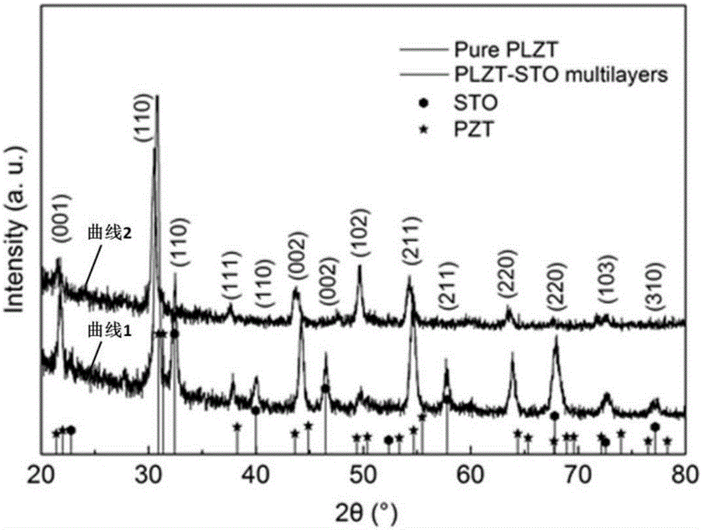
[0053] (1) XRD diffraction comparison chart

[0054] see figure 1 , which is the XRD diffraction diagram of the antiferroelectric PLZT-paraelectric STO coupling film and the pure PLZT film, where curve 1 is the XRD diffraction pattern of the antiferroelectric PLZT-paraelectric STO coupling film, and curve 2 is the pure antiferroelectric PLZT film The XRD diffraction pattern. The test result is obtained by X-ray diffractometer (X'Pert PRO, PANalytical). It can be seen from the figure that the coupled PLZT and STO can form independent phases without any other impurity phases.

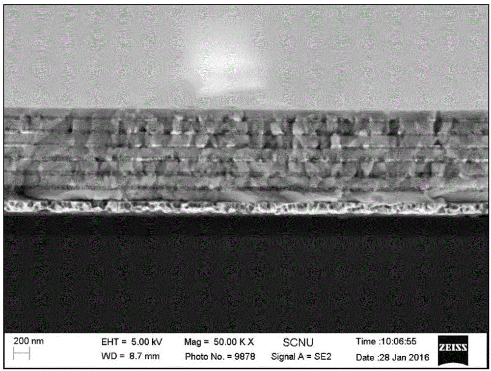
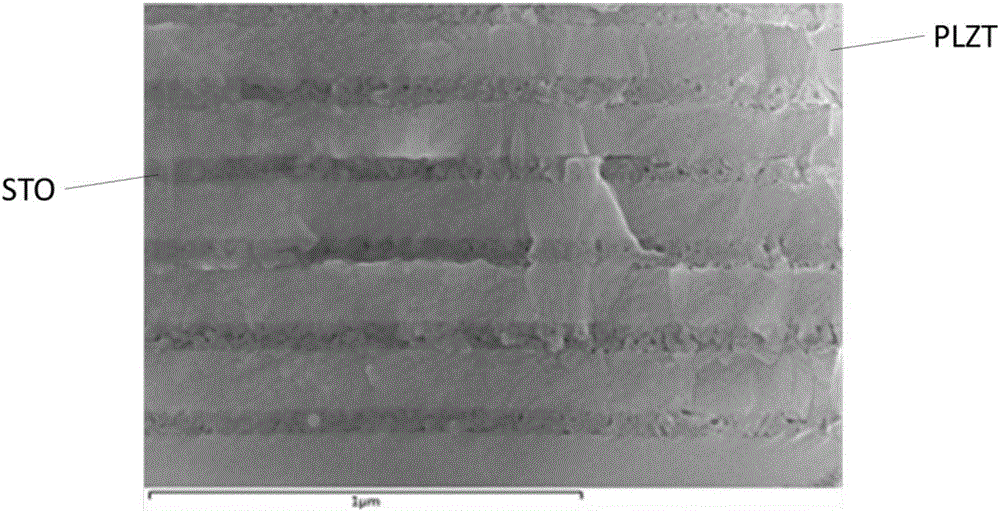
[0055] (2) SEM cross-sectional representation

[0056] Please also see figure 2 and image 3 , figure 2 SEM cross-sectional characterization diagram of antiferroelectric PLZT-paraelectric STO coupling film, image 3 for figure 2 A partial enlar...


PUM


Abstract

The invention discloses an anti-ferroelectric-paraelectric material coupled capacitor dielectric and a preparation method therefor. The anti-ferroelectric-paraelectric material coupled capacitor dielectric is formed by anti-ferroelectric PLZT and paraelectric STO which are distributed at intervals; the preparation method comprises the following steps of preparing PLZT sol and STO sol; uniformly performing spin coating on a Pt / Si substrate with the PLZT sol or the STO sol by a spin coater to obtain a first coating film layer; performing drying and annealing to obtain a first coating layer; performing spin coating on the first coating layer with the STO sol or the PLZT sol by the spin coater to obtain a second coating film layer; performing drying and annealing to obtain a second coating layer; and alternately performing the spin coating and annealing processes of the PLZT sol and the STO sol to obtain the anti-ferroelectric-paraelectric material coupled capacitor dielectric which is formed by anti-ferroelectric PLZT and paraelectric STO that are distributed at intervals. By virtue of the anti-ferroelectric PLZT-paraelectric STO coupling structure, the shortcoming of the poor voltage resistance of the pure anti-ferroelectric PLZT is effectively overcome, and the energy storage density and the energy storage efficiency of the capacitor dielectric are improved.

Description

technical field [0001] The invention relates to the field of capacitors, in particular to a capacitor dielectric coupled with antiferroelectric-paraelectric materials and a preparation method thereof. Background technique [0002] High-energy pulse capacitors can provide a discharge power much greater than that of batteries, but limited by the limited energy storage density, most of the capacitors currently on the market are ceramic capacitors, which are huge and difficult to meet the requirements of device miniaturization. The research of new dielectric materials is beneficial to improve the energy storage density of dielectric materials and withstand higher voltages, so as to realize the miniaturization and convenience of capacitors and expand their application range. [0003] Research on new capacitor materials emerges in an endless stream, mainly including research on ceramics and thick films doped with lead zirconate titanate series elements, research on organic ferroel...

Claims


Application Information

Patent Timeline
IPC IPC(8): H01G4/12
CPCH01G4/1227H01G4/1245
Inventor 曾敏刘聪陆旭兵高兴森刘俊明
Owner SOUTH CHINA NORMAL UNIVERSITY
Why Eureka
Try Eureka