Ga2O3 nerve bionic layer-based nerve bionic device and preparation method thereof

A neural and bionic technology, applied in the direction of electrical components, etc., can solve the problems of poor stability of devices, poor continuity of high and low resistance state conversion, etc., and achieve the effect of good characteristics, high repeatability and stable performance

Active Publication Date: 2017-03-22
HEBEI UNIVERSITY
View PDF6 Cites 0 Cited by
  • Summary
  • Abstract
  • Description
  • Claims
  • Application Information

AI Technical Summary

Problems solved by technology

[0005] The purpose of the present invention is to provide a Ga-based 2 o 3 A neurobionic device of a neurobionic layer and a preparation method thereof, to solve problems such as poor continuity of switching between high and low resistance states and poor device stability in existing neurobionic devices when a voltage is applied

Method used


Image

  • Ga2O3 nerve bionic layer-based nerve bionic device and preparation method thereof
  • Ga2O3 nerve bionic layer-based nerve bionic device and preparation method thereof
  • Ga2O3 nerve bionic layer-based nerve bionic device and preparation method thereof

Examples


Embodiment 1

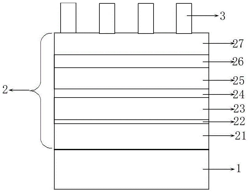
[0036] The neurobionic device provided by the present invention has a structure such as figure 1 shown, including the bottom layer of Pt / Ti / SiO 2 / Si substrate 1, neurobionic layer 2 on the substrate 1, Ag electrode layer 3 on the neurobionic layer 2. Its neurobionic layer 2 is located on the Pt film layer of the substrate 1 .

[0037] Among them, the neurobionic layer 2 is composed of seven layers of film layers stacked in sequence, and from bottom to top is the first Ga layer with a film thickness of 3-7nm. 2 o 3 The film layer 21, the first Ag film layer 22 with a film thickness of 1-3nm, and the second Ga film layer with a film thickness of 3-7nm 2 o 3 The film layer 23, the second Ag film layer 24 with a film thickness of 2-4nm, and the third Ga film with a film thickness of 3-7nm 2 o 3 The film layer 25, the third Ag film layer 26 with a film thickness of 3-5nm, and the fourth Ga film layer with a film thickness of 3-7nm 2 o 3 Membrane 27. The total thickness of...

Embodiment 2

[0040] The preparation method of the neural bionic device provided by the present invention comprises the following steps:

[0041] 1. Forming a neurobionic layer on a substrate

[0042] (1) Prepare the substrate

[0043] Choose Pt / Ti / SiO 2 / Si as the substrate, then Pt / Ti / SiO 2 / Si substrate is placed in acetone and ultrasonically cleaned for 10 minutes, then placed in alcohol and ultrasonically cleaned for 10 minutes, then taken out with clips, placed in deionized water and ultrasonically cleaned for 5 minutes, finally taken out, and cleaned with N 2 blow dry.

[0044] (2) Put the substrate into the chamber and evacuate it

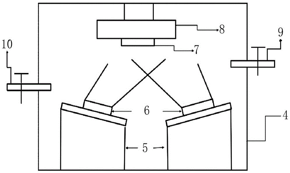
[0045] use as figure 2 For the magnetron sputtering equipment shown, open the chamber 4 of the magnetron sputtering equipment, take out the tablet press table 7, polish it with sandpaper to remove surface stains, clean the polished waste and organic matter attached to the surface with acetone, and finally wipe it with alcohol clean. The cleaned P...

Embodiment 3

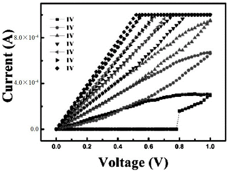
[0069] The neurobionic device prepared in Example 2 was scanned by applying seven positive voltages of 0-1-0V successively, and the results were as follows: image 3 shown. When seven voltage scans of 0-1-0V are applied sequentially to the Ag electrode layer of the neurobionic device prepared in Example 2, when the first voltage scan is applied, when the voltage reaches 0.8v, the resistance of the neurobionic device begins Changes occur, and a steady state can occur. By continuously applying the scanning voltage, the bionic device can realize the memory function, that is, the starting resistance value of a new scanning is the end resistance value of the previous scanning.

[0070] Seven different negative voltages were applied sequentially to the neurobionic device prepared in Example 2 to scan, and the results were as follows: Figure 4 shown. When seven different negative voltage scans are applied to the Ag electrode layer of the neurobionic device prepared in Example 2, ...


PUM


Abstract

The invention discloses a Ga2O3 nerve bionic layer-based nerve bionic device, which comprises a Pt/Ti/SiO2/Si substrate, a nerve bionic layer and an Ag electrode layer, wherein the nerve bionic layer and the Ag electrode layer are sequentially formed on a Pt film of the Pt/Ti/SiO2/Si substrate; and the nerve bionic layer sequentially comprises a first Ga2O3 film, a first Ag film, a second Ga2O3 film, a second Ag film, a third Ga2O3 film, a third Ag film and a fourth Ga2O3 film from bottom to top. Meanwhile, the invention further discloses a preparation method of the nerve bionic device. According to the prepared device, the resistance can be changed according to a time difference between a presynaptic stimulus and a postsynaptic stimulus, the characteristic of a biological synapse can be simulated, high-and-low resistance states slowly change and the range is stable; multiple stable resistance states appear, the nerve bionic device has a good retention characteristic, the resistance can keep relatively high repeatability of high-and-low resistance transformation under the condition of repeatedly exerting electric pulse stimuli; and the nerve bionic device is the nerve bionic device which is more stable in performance and wider in application prospect.

Description

technical field [0001] The invention relates to the technical field of microelectronic devices, in particular to a Ga-based 2 o 3 A neurobionic device of a neurobionic layer and a preparation method thereof. Background technique [0002] In the field of information technology, reducing the area of ​​memory cells is a major driving force in the development of current data storage technologies. However, within the next 15 to 20 years, current storage technologies will reach their physical limits, making further development difficult. In order to promote the sustainable development of storage technology, a new development direction needs to be found. One of its possible development directions is the cognitive storage derived from biological bionics. Unlike the current memory, which only has the single function of data storage, it is as rich and colorful as human memory, which can realize data storage and information processing. And the most important cognitive functions, su...

Claims


Application Information

Patent Timeline
Patent Type & Authority Applications(China)
IPC IPC(8): H01L45/00
CPCH10N70/841H10N70/881H10N70/026H10N70/8833
Inventor 闫小兵赵建辉赵孟柳
Owner HEBEI UNIVERSITY
Why Eureka
Try Eureka