

Transistor and forming method thereof
A technology of transistors and semiconductors, applied in semiconductor devices, semiconductor/solid-state device manufacturing, electrical components, etc., can solve problems such as transistor performance needs to be improved, and achieve the effect of improving position accuracy
- Summary
- Abstract
- Description
- Claims
- Application Information
AI Technical Summary
Problems solved by technology
Method used
Image

Examples
Embodiment Construction
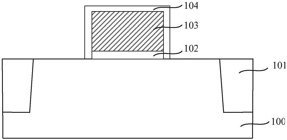
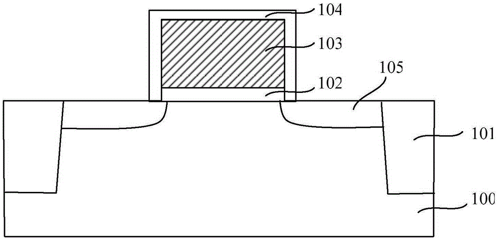
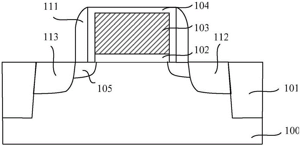
[0037] As mentioned in the background art, the performance of transistors formed in the prior art still needs to be improved. For example, when a transistor is used as a switching device, the switching rate and switching loss of the transistor are two important indicators for evaluating the performance of the transistor. When switching devices, there are still problems such as slow switching speed and large switching loss.
[0038] Studies have found that the switching rate and switching loss of a transistor are closely related to the parasitic capacitance between the drain and channel regions of the transistor, the parasitic capacitance between the source region and the channel region or the parasitic capacitance between the drain and the channel region The larger , the slower the switching rate of the transistor and the greater the switching losses. Further research on the formation process of transistors in the prior art has found that there are two main reasons for the lar...
PUM
| Property | Measurement | Unit |
|---|---|---|
| Thickness | aaaaa | aaaaa |
| Depth | aaaaa | aaaaa |
| Depth | aaaaa | aaaaa |
Abstract
Description
Claims
Application Information