Chip hot layout method

A chip and layout technology, applied in special data processing applications, instruments, electrical digital data processing, etc., can solve problems such as long optimization process, long time, and irregular coding, so as to improve performance and reliability, and reduce hot spot temperature , the effect of reducing the temperature difference

Active Publication Date: 2017-04-26
NORTHEASTERN UNIV
View PDF2 Cites 16 Cited by
  • Summary
  • Abstract
  • Description
  • Claims
  • Application Information

AI Technical Summary

Problems solved by technology

In the articles "Thermal Placement Design for MCM Applications" and "Integration of simulation and response surfacemethods for thermal design of multichip modules", the genetic algorithm is used to optimize the layout of electronic components on the PCB, but this method requires more Storage space, because it must remember all the individual structures in the billion population, and there are problems of non-standard coding and inaccurate coding representation
In addition, the genetic algorithm has no effective quantitative analysis method for the accuracy, feasibility, and computational complexity of the algorithm.
[0007] In the article "Object-Oriented Thermal Placement Using an Accurate Heat Model", the simulated annealing algorithm is used. The optimization process of this algorithm is too long and takes a lot of time, and the solution to a specific problem requires more difficult parameter adjustments. , and it is not necessarily possible to find the global optimal solution
Also, as the article shows, the method does not include boundary setting conditions
[0008] In the article "Optimization of electronics component placement design on PCBusing self organizing genetic algorithm (SOGA)", although this method has better convergence effect, it also requires more processing time

Method used


Image

  • Chip hot layout method
  • Chip hot layout method
  • Chip hot layout method

Examples


Embodiment Construction

[0054] The specific implementation manners of the present invention will be described in detail below in conjunction with the accompanying drawings.

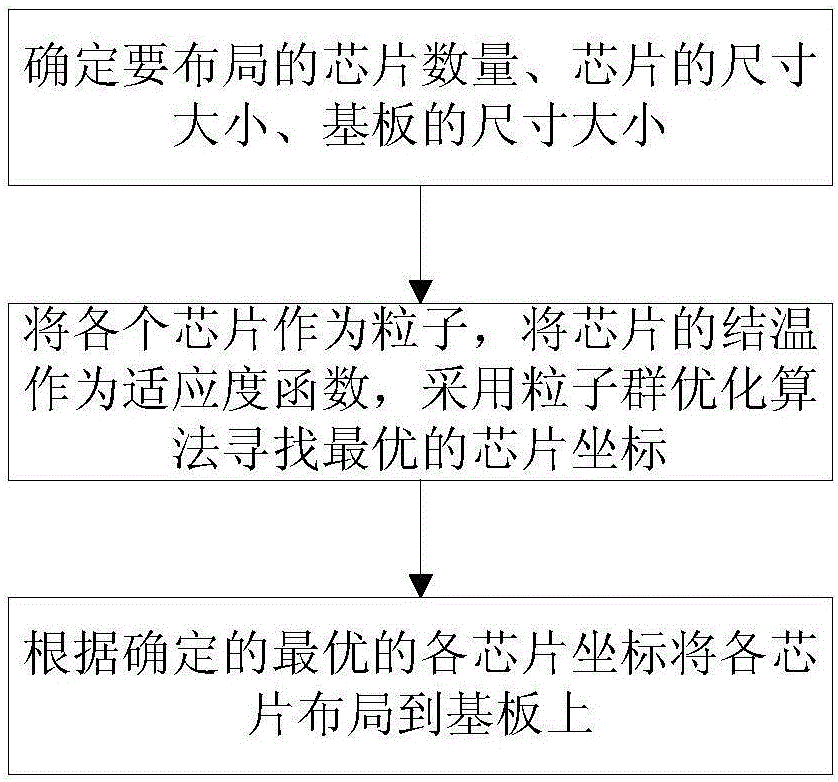
[0055] A chip thermal layout method based on the combination of particle swarm optimization and junction temperature, such as figure 1 shown, including:

[0056] Step 1. Determine the number of chips to be laid out, the size of the chips, and the size of the substrate;

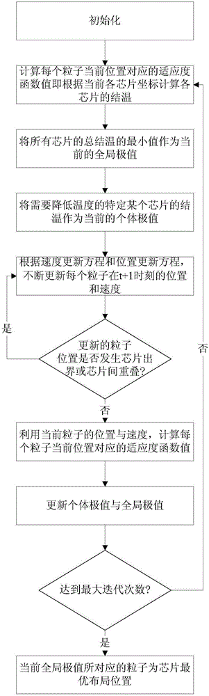
[0057] Step 2. Use each chip as a particle, and all chips on the substrate form a particle swarm, use the junction temperature of the chip as a fitness function, and use the particle swarm optimization algorithm to find the optimal chip coordinates;

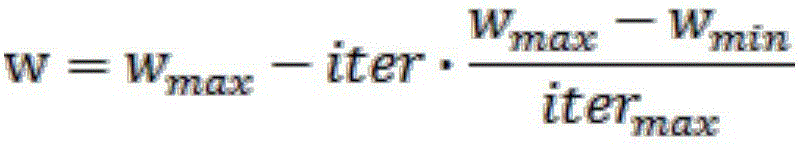
[0058] The particle swarm optimization algorithm is simpler than the rules of the genetic algorithm. It does not have the crossover, mutation and reversal operations of the genetic algorithm, but determines the search direction and step size according to its own speed, and has memory capabilities. The model is sim...


PUM


Abstract

The present invention provides a particle swarm optimization and junction temperature combination-based chip hot layout method. The method comprises the steps of determining a number and sizes of chips to be distributed, and a size of a baseboard; using each chip as a particle, wherein all chips on the baseboard form a particle swarm, using a junction temperature of the chip as a fitness function, and seeking optimal chip coordinates by using a particle swarm optimization algorithm; and distributing each chip on the baseboard according to the determined optimal coordinates of each chip. In the method, the junction temperature of any chip can be designated as the fitness function by taking the advantage of the particle swarm optimization algorithm, the actual size of the chip is taken into account so as to prevent the chip to be out of the bound and overlap, so that all chips on the baseboard are distributed reasonably, further, temperature of a certain high-power chip, a chip not resisting high temperature, or a chip with special requirements reaches a minimum level as much as possible, therefore, hot-spot temperature on the whole baseboard is further reduced, a temperature difference of chips is reduced, and the performance and reliability of the device are improved.

Description

technical field [0001] The invention belongs to the technical field of chip thermal layout, in particular to a chip thermal layout method. Background technique [0002] The traditional thermal layout includes the thermal orientation method, the combination of the micro-element thermal balance method and the optimization method, and other layout methods. [0003] In the articles "Thermal Layout Optimization of Electronic Components on PCB Based on Particle Swarm Algorithm" and "Research on Thermal Layout Optimization of Electronic Components on PCB Based on Ant Colony Algorithm", both methods use the microelement volume thermal balance method to establish The temperature distribution model, however, the micro-element body heat balance method needs to derive various corresponding node equations separately. In the case of complex temperature field and convection, it cannot accurately express the steady-state temperature value corresponding to each chip, and the two This method...

Claims


Application Information

Patent Timeline
Patent Type & Authority Applications(China)
IPC IPC(8): G06F17/50
CPCG06F30/392G06F2119/08
Inventor 杨杰张秀娟章少宇叶柠苑振宇沈鸿媛马文鹏
Owner NORTHEASTERN UNIV
Why Eureka
Try Eureka