Gallium-nitride field effect transistor and manufacturing method therefor

A gallium nitride field and transistor technology, which is applied in semiconductor/solid-state device manufacturing, semiconductor devices, electrical components, etc., can solve the problems of high electric field density and easy breakdown, and achieve the effect of reducing electric field density and improving withstand voltage

Inactive Publication Date: 2017-04-26
PEKING UNIV +2
View PDF4 Cites 34 Cited by
  • Summary
  • Abstract
  • Description
  • Claims
  • Application Information

AI Technical Summary

Problems solved by technology

However, in the traditional field plate structure, the electric field density between the first field plate and the drain is very large, and it is easy to break down.

Method used


Image

  • Gallium-nitride field effect transistor and manufacturing method therefor
  • Gallium-nitride field effect transistor and manufacturing method therefor
  • Gallium-nitride field effect transistor and manufacturing method therefor

Examples


Embodiment Construction

[0036] The technical solutions in the embodiments of the present invention will be clearly and completely described below in conjunction with the accompanying drawings in the embodiments of the present invention. Obviously, the described embodiments are only a part of the embodiments of the present invention, rather than all the embodiments. Based on the embodiments of the present invention, all other embodiments obtained by those of ordinary skill in the art without creative work shall fall within the protection scope of the present invention.

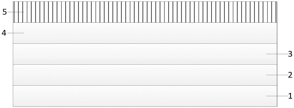
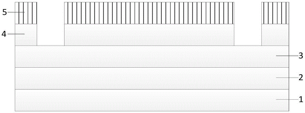
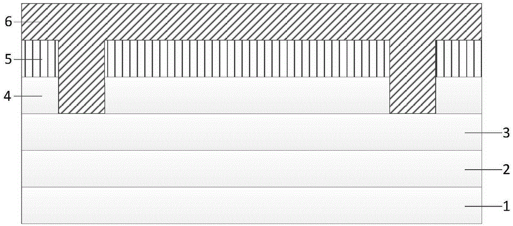
[0037] Figure 8 Shows a schematic structural diagram of a gallium nitride field effect transistor provided by an embodiment of the present invention, such as Figure 8 As shown, the field-effect transistor includes a substrate 1, an epitaxial layer (2 and 3) sequentially formed on the substrate 1, a passivation layer 4, a first oxide layer 5, a source 61, a drain 62, a gate Pole 7, second oxide layer 8 and field plate layer 9.

[0038] Wh...


PUM


Abstract

The invention provides a gallium-nitride field effect transistor, and the field effect transistor comprises a substrate, an epitaxial layer, a passivation layer, a first oxidation layer, a source electrode, a drain electrode, a grid electrode, a second oxidation layer and a field plate layer, wherein the epitaxial layer, the passivation layer, the first oxidation layer, the source electrode, the drain electrode, the grid electrode, the second oxidation layer and the field plate layer are sequentially formed on the substrate. The field plate layer is electrically connected with the source electrode through a metal lead, and is partly opposite to the grid electrode. The invention also provides a manufacturing method for the gallium-nitride field effect transistor. According to the invention, the grid electrode and the field plate layer are arranged to be partly opposite, so the current collapse can be inhibited so as to improve the breakdown characteristics of a device. Moreover, the electric field density between the first field plate layer and the drain electrode can be reduced, thereby improving the withstand voltage of the device.

Description

Technical field [0001] The invention relates to the technical field of semiconductor device manufacturing, in particular to a gallium nitride field effect transistor and a manufacturing method thereof. Background technique [0002] With the increasing demand for efficient and complete power conversion circuits and systems, power devices with low power consumption and high-speed characteristics have recently attracted a lot of attention. Gallium nitride GaN is the third-generation wide-bandgap semiconductor material. Due to its large forbidden band width (3.4eV), high electron saturation rate (2e7cm / s), and high breakdown electric field (1e10--3e10V / cm), it is more High thermal conductivity, corrosion resistance and radiation resistance. It has strong advantages under high-voltage, high-frequency, high-temperature, high-power and radiation-resistant environmental conditions. It is considered to be the most researched short-wave optoelectronic device and high-voltage high-frequency...

Claims


Application Information

Patent Timeline
Patent Type & Authority Applications(China)
IPC IPC(8): H01L29/78H01L29/06H01L29/40H01L29/20H01L21/336
CPCH01L29/78H01L29/0611H01L29/2003H01L29/402H01L29/66477
Inventor 刘美华陈建国林信南
Owner PEKING UNIV
Why Eureka
Try Eureka