Method for monitoring silicon chip injection temperature

A silicon wafer and post-implantation technology, applied in semiconductor/solid-state device testing/measurement, electrical components, circuits, etc., can solve problems such as unable to monitor ion implantation

Inactive Publication Date: 2017-05-10
SHANGHAI HUAHONG GRACE SEMICON MFG CORP
View PDF5 Cites 2 Cited by
  • Summary
  • Abstract
  • Description
  • Claims
  • Application Information

AI Technical Summary

Problems solved by technology

This patent does not need to analyze and shape the extracted ion beam, which reduces the price of the i...

Method used


Image

  • Method for monitoring silicon chip injection temperature
  • Method for monitoring silicon chip injection temperature
  • Method for monitoring silicon chip injection temperature

Examples


Embodiment Construction

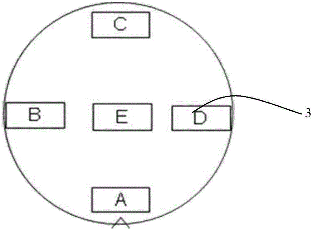
[0038] Such as image 3 As shown, polysilicon is a commonly used material in semiconductor manufacturing. Its manufacturing cost is low, and it can be grown by CVD (chemical vapor deposition), with good uniformity and high yield; polysilicon film can be peeled off by wet chemical solution tank and then Growing, silicon wafers can be recycled and used repeatedly.

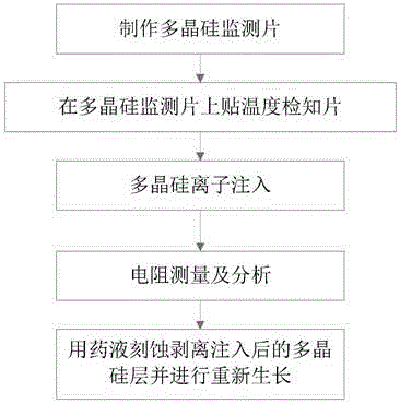
[0039] Such as Figure 6 As shown, the method for monitoring the temperature of implanted silicon wafer in a preferred embodiment of the present invention comprises the following steps:

[0040] Step 1, making a polysilicon monitoring chip. Deposit a layer of silicon oxide on the silicon substrate, and then grow a layer of 3000 angstrom polysilicon layer. The polysilicon layer can be grown by CVD (chemical vapor deposition). The working temperature of the chemical vapor deposition method can be controlled between 500°C and 700°C. Polysilicon ions are uniformly deposited on the oxide layer in the physical vapor dep...


PUM

PropertyMeasurementUnit
Thicknessaaaaaaaaaa

Abstract

The invention discloses a method for monitoring silicon chip injection temperature. The method is realized by measuring resistance of a silicon chip having a polycrystalline silicon layer. Polycrystalline silicon injection is very sensitive to temperature, and a channel effect of ions on polycrystalline silicon is far smaller than that on monocrystalline silicon, so that amorphous phenomenon in injection is more obvious, and the injection is more sensitive to heat generated after ionic bombardment, which can be directly reflected on polysilicon resistance; and through the theories above, correlation between the polysilicon resistance and temperature in corresponding injection can be established, and actual injection temperature can be monitored based on the resistance. Therefore, the method for monitoring the silicon chip injection temperature is realized by measuring the resistance of the silicon chip having the polycrystalline silicon layer.

Description

technical field [0001] The invention relates to the technical field of designing semiconductor devices, in particular to a method for monitoring the temperature of implanted silicon wafers. Background technique [0002] In VLSI manufacturing, ion implantation technology has been more and more widely used. The silicon wafer with patterned devices on the surface is heated by the bombardment of a large number of ions during the process, resulting in a gradual increase in temperature; if the heat cannot be taken away in time, it will affect the electrical properties of the doping, and even lead to the formation of photoresist morphology. Changes occur, and the photolithography pattern is deformed. At this time, performing ion implantation with the deformed photolithographic pattern will result in a device with abnormal parameters, which will cause the failure of the semiconductor process. [0003] At the same time, the injected target disk is cooled by circulating cooling wate...

Claims


Application Information

Patent Timeline
IPC IPC(8): H01L21/66
CPCH01L22/12
Inventor 郑刚陈立鸣
Owner SHANGHAI HUAHONG GRACE SEMICON MFG CORP
Why Eureka
Try Eureka