BSI CMOS image sensor with improved phase detecting pixel

An image sensor and phase detection technology, applied in the field of image sensors, can solve problems such as phase detection capability degradation

Active Publication Date: 2017-05-10
OMNIVISION TECH INC
View PDF4 Cites 6 Cited by
  • Summary
  • Abstract
  • Description
  • Claims
  • Application Information

AI Technical Summary

Problems solved by technology

[0004] Compared to BSI CMOS image sensors fabricated with BCFA, higher quantum efficiency (QE) can be achieved with BSI CMOS image senso

Method used


Image

  • BSI CMOS image sensor with improved phase detecting pixel
  • BSI CMOS image sensor with improved phase detecting pixel
  • BSI CMOS image sensor with improved phase detecting pixel

Examples


Embodiment Construction

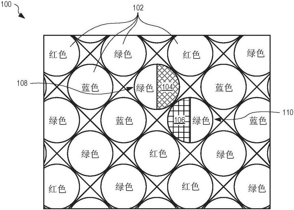
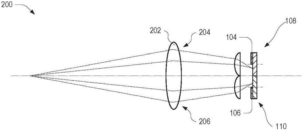
[0016] figure 1 A pixel pattern is shown for a backside illuminated (BSI) complementary metal oxide semiconductor (CMOS) image sensor 100 having a plurality of pixels 102 each having a color filter and a lens, where two pixels are each configured with a right phase detection pixel (PDP) mask 104 and left PDP mask 106 to operate as PDPs 108 and 110 . figure 2 is showing figure 1 A schematic diagram of an exemplary operation of the PDP 108 to detect light from the first side 204 of the objective lens 202 and an exemplary operation of the PDP 110 to detect light from the second side 206 of the objective lens 202 . Phase detection pixels 108, 110 may be used within the camera to improve autofocus by detecting differences in phase with respect to the focus of the object being captured. The cameras adjust focus to align with the detected phases from PDPs 108 and 110 .

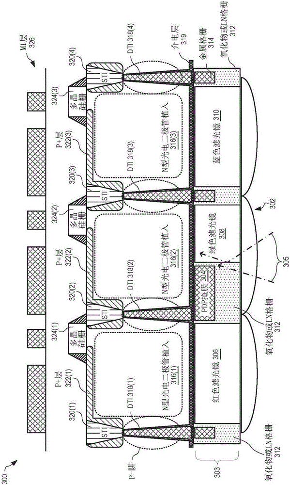
[0017] 3 is a cross-section of part of a related art BSI CMOS image sensor 300 showing the structure of a rela...


PUM


Abstract

An improved back side illuminated (BSI) complementary metal oxide semiconductor (CMOS) image sensor, and associated methods, improve phase detecting capability. The BSI CMOS image sensor has an array of pixels that include a phase detecting pixel (PDP), a composite grid formed of a buried color filter array and composite metal/oxide grid, and a photodiode implant corresponding to the PDP. A PDP mask is fabricated with a deep trench isolation (DTI) structure proximate the PDP and positioned to mask at least part of the photodiode implant such that the PDP mask is positioned between the composite grid and the photodiode implant.

Description

technical field [0001] The present disclosure relates to the technical field of image sensors, in particular to a BSICMOS image sensor with improved phase detection pixels. Background technique [0002] Phase detection pixels (PDPs) on backside illuminated (BSI) complementary metal oxide semiconductor (CMOS) image sensors are useful for improving focus in cameras. Paired pixels are masked such that they only detect light from one or the other edge of the objective. Pairs of complementary PDPs are placed on the sensor to allow the camera to determine how light is received out of phase at the current location, thereby determining the lens focus adjustments needed to focus the image on the sensor. [0003] Conventional BSI CMOS image sensor fabrication with PDP forms a PDP mask for each PDP when forming a metal grid that also includes a composite grid (oxide on metal) layer of a buried color filter array (BCFA). Therefore, the PDP mask is also arranged within the composite gr...

Claims


Application Information

Patent Timeline
IPC IPC(8): H01L27/146
CPCH01L27/14605H01L27/14614H01L27/14625H01L27/14643H01L27/14627H01L27/14645H01L27/1464H01L27/14621H01L27/1463H01L27/14609H01L27/14685H01L27/14683
Inventor 刘家颖彭进宝熊志伟威尼斯·文森特
Owner OMNIVISION TECH INC
Why Eureka
Try Eureka