Temperature sensing diode structure integrated on transistor and preparation method thereof

A diode and transistor technology, applied in the field of temperature sensing diode structure and its preparation, can solve the problems of incomplete compatibility of transistor process, increase production cost, complex structure of power semiconductor module, etc., and achieve improved anti-interference ability, reliability, safety work, avoid the effect of the inductive effect

Active Publication Date: 2017-05-24
MACMIC SCIENCE & TECHNOLOGY CO LTD
View PDF5 Cites 8 Cited by
  • Summary
  • Abstract
  • Description
  • Claims
  • Application Information

AI Technical Summary

Problems solved by technology

On the other hand, the polycrystalline thin film diode also needs to be connected to the transistor through an internal circuit, resulting in a complex structure of the power semiconductor module, and it is not fully compatible with transistor processes such as IGBT and MOSFET, which increases the production cost

Method used


Image

  • Temperature sensing diode structure integrated on transistor and preparation method thereof
  • Temperature sensing diode structure integrated on transistor and preparation method thereof
  • Temperature sensing diode structure integrated on transistor and preparation method thereof

Examples


Embodiment Construction

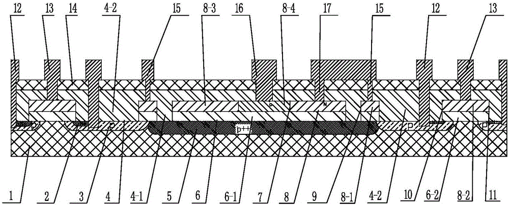
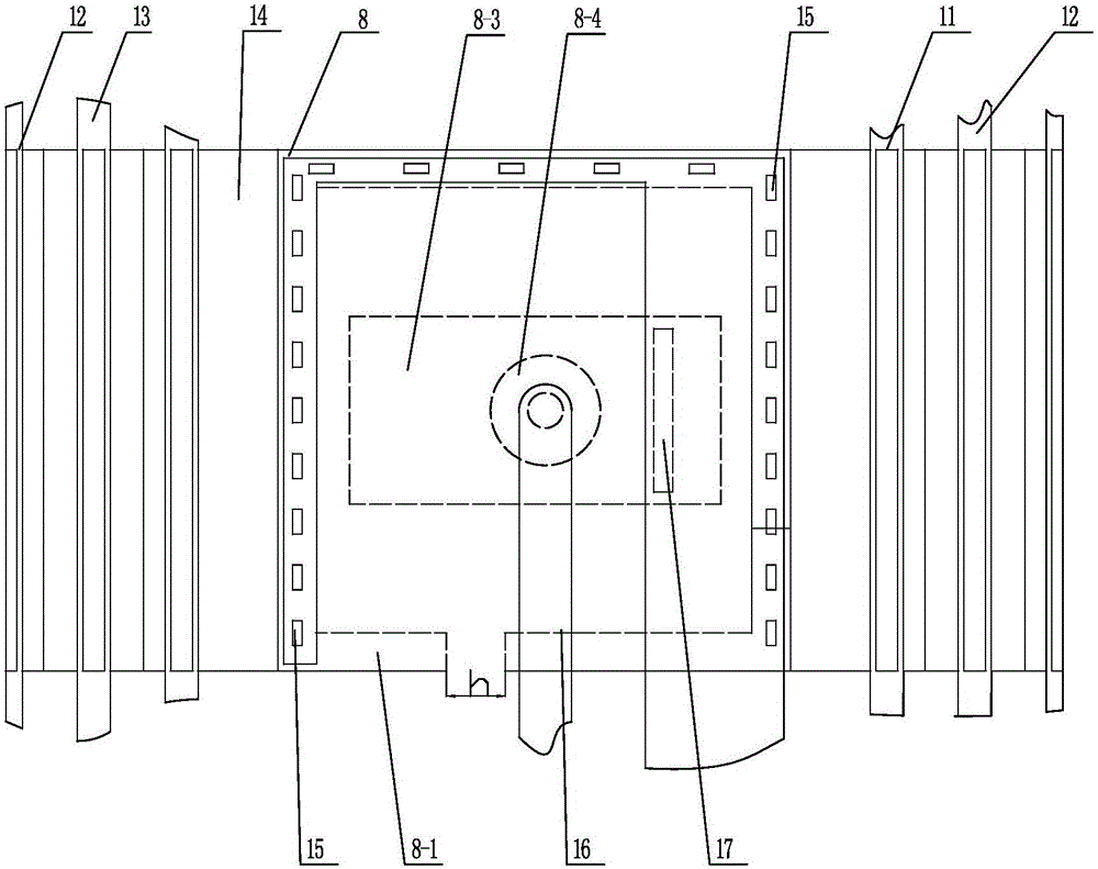
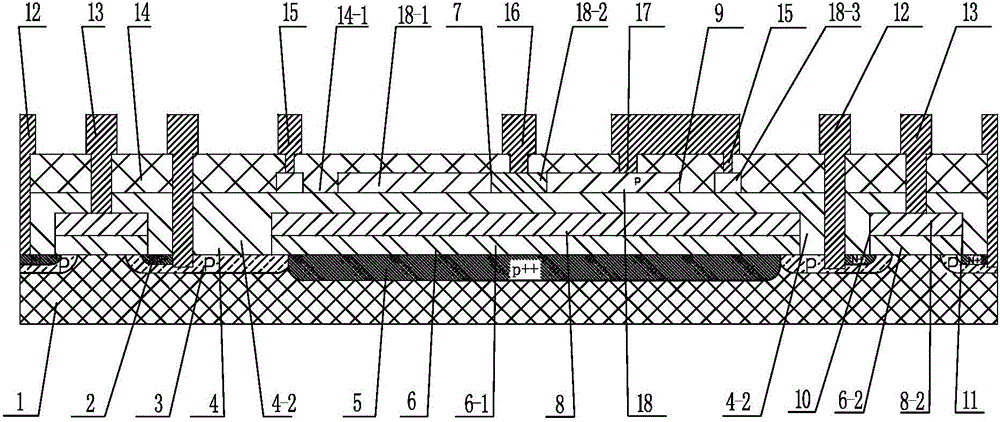
[0044] See figure 1 , 2 As shown, in the temperature sensing diode structure integrated on the transistor of the present invention, the active area of ​​the silicon chip 1 is connected with the first oxide layer 6 and the first polysilicon layer 8 on it in sequence, and the first oxide layer 6 As the isolation layer 6-2 of the polysilicon gate 8-2, the first polysilicon layer 8 is the polysilicon gate 8-2 of the transistor, and the silicon chip 1 has a first doped layer connected to the silicon chip 1 in the source cell of the active region. The impurity region 3 is connected to the second doped region 2 in the first doped region 3, the emitter 12 is connected to the first doped region 3 and the second doped region 2, and the gate 13 is connected to the polysilicon gate 8-2 , and the first polysilicon layer 8 is treated as the first doped region 8-3 of the diode of the present invention, and the upper part of the first polysilicon layer 8 is connected with the second oxide la...


PUM

PropertyMeasurementUnit
thicknessaaaaaaaaaa

Abstract

The invention relates to a temperature sensing diode structure integrated on a transistor and a preparation method thereof; the upper portion of a first polysilicon layer is connected with a second oxide layer and an insulation dielectric layer; the second oxide layer has an isolation portion isolating a diode zone and an annular isolation portion; the annular isolation portion can isolate the first polysilicon layer in the diode zone so as to form a diode first doping zone and an isolation protection ring separated from each other; the isolation protection ring is not closed; a diode second doping zone with an arced periphery is connected in the diode first doping zone so as to form a transverse PN junction; the first and second electrodes of the diode are connected with corresponding first and second doping zones of the diode; a protection electrode penetrates the insulation dielectric layer and is connected with the isolation protection ring on the first polysilicon layer; the protection electrode is connected with the first electrode so as to form equipotential. The temperature sensing diode structure is reasonable in structure, can detect the transistor chip temperature in real time, can prevent external current, voltage and electric field changes from affecting the temperature sensing diode, and can reduce the production cost.

Description

technical field [0001] The invention relates to a temperature sensing diode structure integrated on a transistor and a preparation method thereof, belonging to the technical field of transistor production. Background technique [0002] High-current, high-power power semiconductor modules are increasingly used in the automotive field, and protection measures such as over-temperature, over-current, and over-voltage are required for insulated-gate bipolar transistors (IGBTs) or field-effect transistors (MOSFETs). An IGBT or MOSFET needs to be integrated with a temperature sensor. Through the integrated temperature sensor, the temperature of the module and chip can be detected effectively in real time, so as to protect the device in time. At present, most power semiconductor modules package the temperature sensitive element and IGBT or MOSFET chip in the same module, and the temperature sensitive element is to detect the temperature of the circuit and convert the temperature si...

Claims


Application Information

Patent Timeline
Patent Type & Authority Applications(China)
IPC IPC(8): H01L23/34H01L29/739H01L21/331G01K7/01
CPCG01K7/01H01L23/34H01L29/66333H01L29/7393
Inventor 王培林井亚会戚丽娜张景超刘利峰赵善麒
Owner MACMIC SCIENCE & TECHNOLOGY CO LTD
Why Eureka
Try Eureka