

Large-area non-aqueous transferring method of nano material
A nanomaterial, water transfer technology, applied in the direction of nanocarbon, nanotechnology, nanotechnology for materials and surface science, etc., to achieve good fidelity effect
- Summary
- Abstract
- Description
- Claims
- Application Information
AI Technical Summary
Problems solved by technology
Method used
Image

Examples
Embodiment Construction
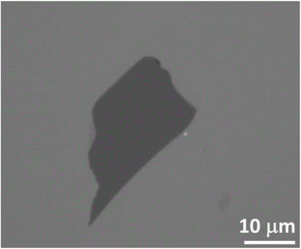
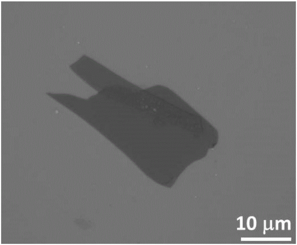
[0023] Attached below Figures 1 to 3 An example of the technical solution of the invention will be described.
[0024] Silicon wafers treated with a plasma cleaning machine, the cleaned silicon wafers are modified in a toluene solution of octadecyltrimethoxysilane at a temperature of 60 degrees Celsius for 12 hours, and a silane-based layer is formed on the surface of the silicon wafers to make the silicon wafers hydrophobic Effect.
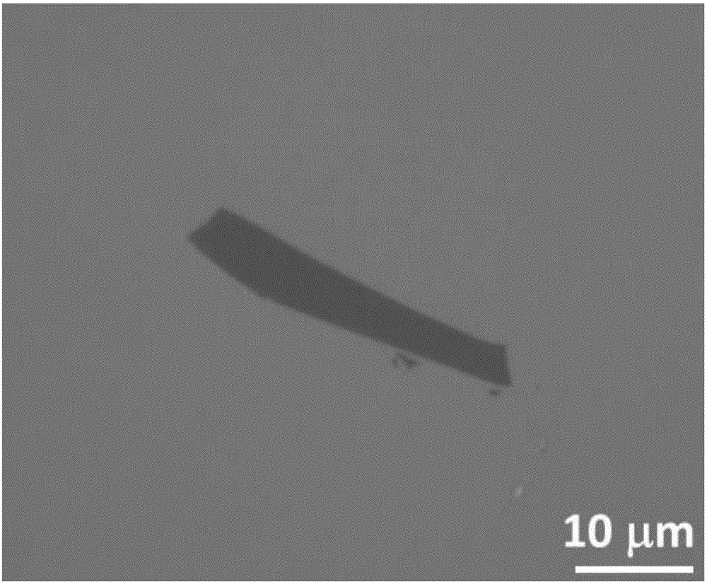
[0025] Tungsten diselenide samples were prepared on modified silicon wafers by mechanical exfoliation, such as figure 1 Shown is a tungsten diselenide sample.
[0026] On the tungsten diselenide material on the silicon wafer, the dichloromethane solution of one deck polymethyl methacrylate is spin-coated, and the mass volume ratio of the dichloromethane solution of polymethyl methacrylate is 3%; Material variance adjustments.
[0027] Cover the film made of polydimethylsiloxane on the polymer film of polymethyl methacrylate formed by spin co...
PUM
 Abstract
Description
Claims
Application Information