
Neural network space mapping modeling method for power transistor

A power transistor and neural network technology, applied in the field of microwave circuit and device modeling, can solve the problems of complex neural network structure, a large number of weight parameters, increase the difficulty of model training, etc., achieve simple neural network structure, reduce the number of iterations, and shorten the construction time. effect of die cycle

Inactive Publication Date: 2017-05-31
TIANJIN POLYTECHNIC UNIV +1
View PDF4 Cites 12 Cited by
  • Summary
  • Abstract
  • Description
  • Claims
  • Application Information

AI Technical Summary

Problems solved by technology

The existing neural network model structure uses the neural network to simultaneously control the DC characteristics and AC characteristics of the device, which will lead to a complex neural network structure, requiring a large number of weight parameters, and increasing the difficulty of model training

Method used


Image

  • Neural network space mapping modeling method for power transistor
  • Neural network space mapping modeling method for power transistor
  • Neural network space mapping modeling method for power transistor

Examples


Embodiment Construction

[0032] In order to make the objectives, technical solutions, and advantages of the present invention clearer, the embodiments of the present invention will be described in detail below in conjunction with the accompanying drawings.

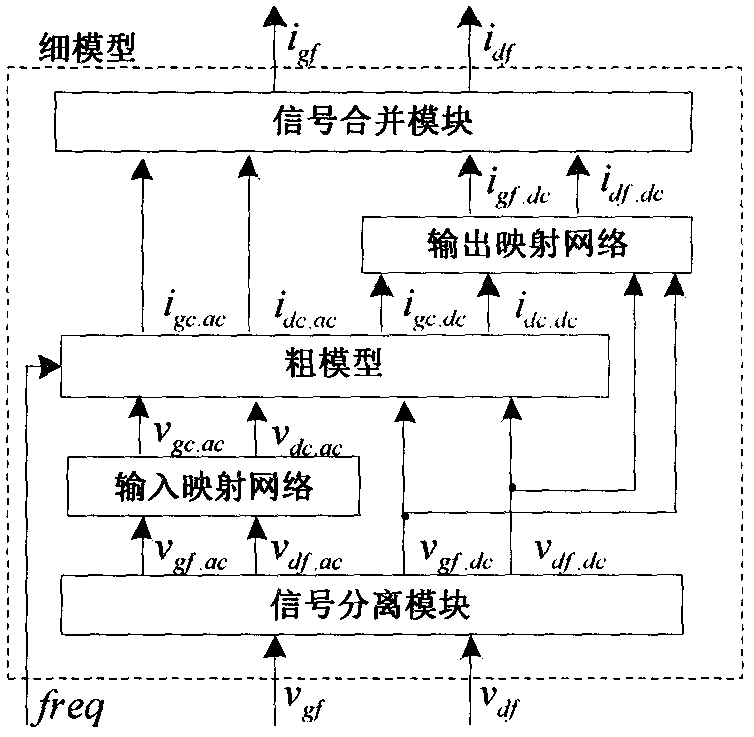
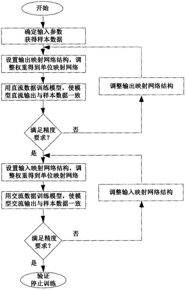
[0033] Such as figure 2 As shown, in a neural network spatial mapping modeling method for power transistors of the present invention, first, sample data for model training must be obtained. The DC input sample data is the input voltage, denoted as [v gf , V df ] T ; The DC output sample data is the output current, denoted as [i df ]. The AC input sample data is the input voltage and frequency, denoted as [v gf , V df , Freq] T ; AC output sample data is S parameter, denoted as [S 11 , S 12 , S 21 , S 22 ] T . The sample data can be obtained through actual measurement devices or simulation software.

[0034] Build as figure 1 As shown in the neural network structure, set the output mapping network structure. The output mapping network uses a 3-la...


PUM


Abstract

The invention belongs to the field of modeling of microwave circuits and devices, and provides a neural network space mapping modeling method for a power transistor. According to the method, a direct current signal and an alternating current signal in an input / output signal of a power transistor model are separately processed, an output mapping network is used to adjust the direct current characteristic of the power transistor model, and an input mapping network is used to adjust the alternating current characteristic of the power transistor model. The method inherits the advantages of the conventional neural network space mapping method, the mutual interference of the parameters on the model performance is reduced, the repeated adjustment and optimization of the parameters is avoided, and the modelling period is shortened.

Description

Technical field [0001] The invention relates to the field of microwave circuit and device modeling, in particular to the application of neural network space mapping technology in the field of microwave modeling. Background technique [0002] In recent years, in order to produce electronic products with higher precision and faster speed, electronic devices with new processes, new materials, and new structures have continuously emerged. With the increase in circuit structure complexity, the reduction of design errors and the shortening of design time cycles, designers often rely on computer-aided design for circuit simulation and verification, causing designers to rely more and more on high-precision and fast-speed device models. The semiconductor device model is the most important factor affecting the accuracy of circuit design. The larger the circuit scale, the higher the index and the frequency band, the higher the requirements for the device model. The device model in the fiel...

Claims


Application Information

Patent Timeline
IPC IPC(8): G06F17/50G06N3/04G06N3/08
CPCG06N3/08G06F30/367G06N3/045
Inventor 闫淑霞靳晓怡赵宝柱赵靖曹宇
Owner TIANJIN POLYTECHNIC UNIV
Learn More