LED epitaxial structure of composite P-type GaN layer and fabrication method of LED epitaxial structure

An epitaxial structure, n-type technology, used in electrical components, circuits, semiconductor devices, etc., can solve the problem of low hole concentration, and achieve the effect of increasing hole concentration, increasing activation rate, improving luminous efficiency and electrical properties

Inactive Publication Date: 2017-05-31
XIANGNENG HUALEI OPTOELECTRONICS
View PDF4 Cites 19 Cited by
  • Summary
  • Abstract
  • Description
  • Claims
  • Application Information

AI Technical Summary

Problems solved by technology

[0005] The purpose of the present invention is to provide a compound P-type GaN layer LED epitaxial structure and its preparation method to solve the technical problem that the hole concentration of the P-type GAN layer GaN structure is not high

Method used


Image

  • LED epitaxial structure of composite P-type GaN layer and fabrication method of LED epitaxial structure
  • LED epitaxial structure of composite P-type GaN layer and fabrication method of LED epitaxial structure
  • LED epitaxial structure of composite P-type GaN layer and fabrication method of LED epitaxial structure

Examples


Embodiment 1

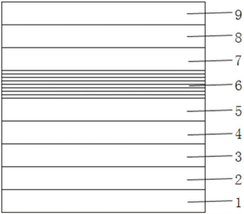
[0053] The concrete steps of this embodiment are as follows:

[0054] 1. Substrate treatment: raise the temperature to 1230-1250°C, and treat the substrate for 4-8 minutes;

[0055] 2. Growth buffer layer: lower the temperature to 520-550°C, 2 growing a buffer layer with a thickness of 20-25 nm on the above substrate under the atmosphere;

[0056] 3. Growing u-type GaN layer: Raise the reaction chamber temperature to 1160-1180°C, 2 Under the atmosphere, grow a 3-3.5 μm thick u-type GaN layer on the above buffer layer;

[0057] 4. Growth of n-type GaN layer: raise the temperature of the reaction chamber to 1240-1260°C, the pressure of the reaction chamber is 550-600mbar, in H 2 Under the atmosphere, grow a 3-3.5 μm thick n-type GaN layer on the above-mentioned u-type GaN layer, and the doping concentration of Si is 8×10 18 ~1.1×10 19 atoms / cm 3 ;

[0058] 5. To grow the MQW active layer: reduce the temperature of the reaction chamber to 900-970°C, 2 Under the atmosphere...


PUM

PropertyMeasurementUnit
thicknessaaaaaaaaaa
thicknessaaaaaaaaaa
thicknessaaaaaaaaaa

Abstract

The invention provides an LED epitaxial structure of a composite P-type GaN layer and a fabrication method of the LED epitaxial structure. The P-type GaN layer of the LED epitaxial structure sequentially comprises a first P-type GaN layer, a second P-type GaN layer and a third P-type GaN layer, wherein the thickness of the first P-type GaN layer is 40-80 nanometers, the thickness of the second P-type GaN layer is 30-70 nanometers, and the thickness of the third P-type GaN layer is 4-10 nanometers. In the P-type GaN layer structure, two effects are achieved by simultaneously doping an n-type dopant and a P-type dopant: the solubility of the dopants (the formation energy of the dopants is reduced) is increased to prevent a self-compensation effect, and the activation ratio is improved by reducing an acceptor level, so that the self-compensation effect of the P-type GaN layer is prevented better, the hole concentration is improved, and the purpose of improving the luminous efficiency and the electricity of a GaN device is achieved.

Description

technical field [0001] The invention relates to the technical field of semiconductor lighting, in particular to an LED epitaxial structure with a composite P-type GaN layer and a preparation method thereof. Background technique [0002] GaN light-emitting diode (LED), as a new type of high-efficiency, environmentally friendly and green solid-state lighting source, has the characteristics of small size, light weight, long life, high reliability and low power consumption, and is widely used in outdoor display screens, car lights, Traffic lights, landscape lighting, backlight and other fields. [0003] The fabrication of GaN devices involves doping issues. GaN doped with Si can easily achieve n-type, and the electron concentration can reach 10. 15 ~10 20 cm 3 , room temperature mobility over 300cm 2 / V·s. However, P-type Mg doping will cause many problems in the production process, and the hole concentration is only 10 17 ~10 18 cm 3 , the mobility is less than 10cm 2 ...

Claims


Application Information

Patent Timeline
Patent Type & Authority Applications(China)
IPC IPC(8): H01L33/00H01L33/32
CPCH01L33/0075H01L33/325
Inventor 刘为刚曾莹
Owner XIANGNENG HUALEI OPTOELECTRONICS
Why Eureka
Try Eureka