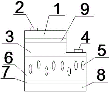
Manufacturing method of invisible cutting and back plating LED chips
A LED chip and invisible cutting technology, which is applied in the direction of electrical components, circuits, semiconductor devices, etc., can solve the problems of unsatisfactory LED luminous efficiency and high shedding rate of the reflective layer, and achieve the effect of improving the effect, improving the light output efficiency and reducing the shedding probability.
- Summary
- Abstract
- Description
- Claims
- Application Information
AI Technical Summary
Problems solved by technology
Method used
Image
Examples
Embodiment 1
[0032] A method for stealth cutting and back-plating LED chips, comprising the following steps:
[0033] a. Growing an adhesion layer: growing an adhesion layer on the back of the wafer;
[0034] b. Film: put the wafer face up and stick the back on the white film;
[0035] c. Stealth dicing: Stealth dicing of the wafer after filming;
[0036] d. Flip: Flip the wafer with the front side down and the back side up on another white film after stealth dicing, and cut off the area where the wafer is located together with the white film.
[0037] e. Metal reflective layer on the back: coat a metal reflective layer on the growth adhesion layer on the back of the wafer;
[0038] f. Splitting: splitting the wafer into single LED chips.
[0039] In step a, an adhesion layer is grown on the backside sapphire substrate of the wafer by PECVD technology, and the adhesion layer is SiO 2 Adhesive layer, the thickness of the adhesive layer is 10nm.
[0040] In step c, during stealth cuttin...
Embodiment 2
[0044] A method for stealth cutting and back-plating LED chips, comprising the following steps:
[0045] a. Growing an adhesion layer: growing an adhesion layer on the back of the wafer;
[0046] b. Film: put the wafer face up and stick the back on the white film;
[0047] c. Stealth dicing: Stealth dicing of the wafer after filming;
[0048] d. Flip: Flip the wafer with the front side down and the back side up on another white film after stealth dicing, and cut off the area where the wafer is located together with the white film.
[0049] e. Metal reflective layer on the back: coat a metal reflective layer on the growth adhesion layer on the back of the wafer;
[0050] f. Splitting: splitting the wafer into single LED chips.
[0051] In step a, an adhesion layer is grown on the backside sapphire substrate of the wafer by PECVD technology, and the adhesion layer is Si 3 N 4 Adhesive layer, the thickness of the adhesive layer is 230nm.
[0052] In step c, during stealth c...
Embodiment 3
[0056] A method for stealth cutting and back-plating LED chips, comprising the following steps:
[0057] b. Film: put the wafer face up and stick the back on the white film;
[0058] c. Stealth dicing: Stealth dicing of the wafer after filming;
[0059] d. Flip: Flip the wafer with the front side down and the back side up on another white film after stealth dicing, and cut off the area where the wafer is located together with the white film.
[0060] e. Metal reflective layer on the back: coat a metal reflective layer on the growth adhesion layer on the back of the wafer;
[0061] f. Splitting: splitting the wafer into single LED chips.
[0062] In step a, an adhesion layer is grown on the backside sapphire substrate of the wafer by PECVD technology, and the adhesion layer is Si 3 N 4 Adhesive layer, the thickness of the adhesive layer is 100nm.
[0063] In step c, during stealth cutting, the laser pulse frequency is 80 Hz, and the scribing speed is 100 mm / s.
[0064] In s...
PUM
| Property | Measurement | Unit |
|---|---|---|
| thickness | aaaaa | aaaaa |
| thickness | aaaaa | aaaaa |
| thickness | aaaaa | aaaaa |
Abstract
Description
Claims
Application Information
 - R&D Engineer
- R&D Manager
- IP Professional
- Industry Leading Data Capabilities
- Powerful AI technology
- Patent DNA Extraction
Browse by: Latest US Patents, China's latest patents, Technical Efficacy Thesaurus, Application Domain, Technology Topic.
© 2024 PatSnap. All rights reserved.Legal|Privacy policy|Modern Slavery Act Transparency Statement|Sitemap

