Bearing substrate for bearing OLED (Organic Light Emitting Diode) during preparation of OLED and preparation method of bearing substrate

A technology for supporting substrates and manufacturing methods, applied in chemical instruments and methods, final product manufacturing, sustainable manufacturing/processing, etc., can solve problems such as exacerbating deformation of glass substrates, shadow effects, and loose bonding between Mask and glass substrates, etc. Achieve the effects of eliminating deformation, avoiding shadow effects, and avoiding vapor deposition and color mixing

Active Publication Date: 2017-05-31
WUHAN CHINA STAR OPTOELECTRONICS SEMICON DISPLAY TECH CO LTD
View PDF7 Cites 4 Cited by
  • Summary
  • Abstract
  • Description
  • Claims
  • Application Information

AI Technical Summary

Problems solved by technology

In the OLED production process, the shrinkage of the flexible substrate after solidification and film formation on the glass substrate will aggravate the deformation of the glass substrate. The deformation of the glass substrate gradually increases from its edge to the center position. When it is attached under the action of a magnet, the Mask and the glass substrate will not be tightly attached, resulting in shadow effects and color mixing

Method used


Image

  • Bearing substrate for bearing OLED (Organic Light Emitting Diode) during preparation of OLED and preparation method of bearing substrate
  • Bearing substrate for bearing OLED (Organic Light Emitting Diode) during preparation of OLED and preparation method of bearing substrate
  • Bearing substrate for bearing OLED (Organic Light Emitting Diode) during preparation of OLED and preparation method of bearing substrate

Examples


Embodiment Construction

[0018] Hereinafter, embodiments of the present invention will be described in detail with reference to the accompanying drawings. This invention may, however, be embodied in many different forms and should not be construed as limited to the specific embodiments set forth herein. Rather, the embodiments are provided to explain the principles of the invention and its practical application, thereby enabling others skilled in the art to understand the invention for various embodiments and with various modifications as are suited to particular intended uses.

[0019] In the drawings, the thicknesses of layers and regions are exaggerated for device clarity. Like reference numerals refer to like components throughout the specification and drawings.

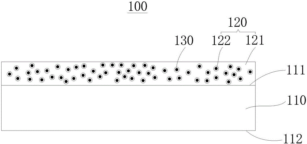
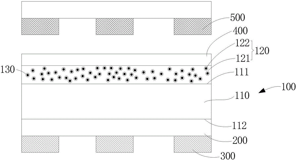
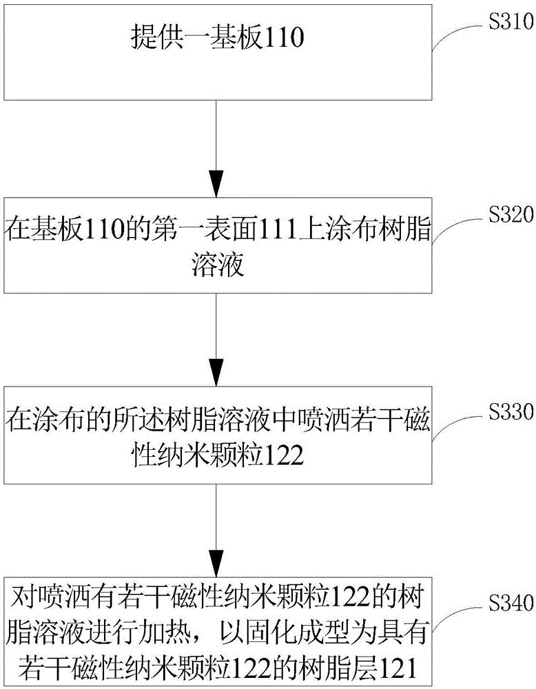
[0020] figure 1 It is a structural schematic diagram of a carrier substrate for carrying OLEDs when manufacturing OLEDs according to an embodiment of the present invention.

[0021] refer to figure 1 , according to an embodiment of t...


PUM

PropertyMeasurementUnit
particle diameteraaaaaaaaaa

Abstract

The invention discloses a bearing substrate for bearing an OLED (Organic Light Emitting Diode) during preparation of the OLED. The bearing substrate comprises a substrate part and an adsorbed layer arranged on the surface of the substrate part, wherein the adsorbed layer comprises a resin layer and a plurality of magnetic nano particles distributed in the resin layer. The invention further discloses a preparation method of the bearing substrate. During the preparation of the OLED, the gravity of the substrate can be counteracted or reduced by an attractive force of an adsorbent to the adsorbed layer, so that deformation caused by gravity sag of the substrate for bearing the OLED during the preparation of the OLED can be eliminated or reduced; and a shadow effect and evaporation color mixture in a preparation process can be further avoided.

Description

technical field [0001] The invention belongs to the field of organic light-emitting technology, and in particular relates to a carrying substrate used for carrying OLEDs when manufacturing OLEDs and a manufacturing method thereof. Background technique [0002] In recent years, Organic Light Emitting Diode (OLED) has become an emerging flat-panel display product at home and abroad, because OLED displays have self-illumination, wide viewing angle (over 175°), short response time (1μs), high luminescence Efficiency, wide color gamut, low operating voltage (3-10V), thin panel (thickness can be less than 1mm), large-size and flexible panels can be produced, and simple manufacturing process, and it also has the potential of low cost. [0003] In the production process of OLED, the glass substrate sags under the influence of gravity in the evaporation machine, thereby causing deformation, and as the size of the glass substrate becomes larger and thinner, the amount of deformation i...

Claims


Application Information

Patent Timeline
Patent Type & Authority Applications(China)
IPC IPC(8): H01L51/56
CPCH10K71/40Y02E10/549C23C14/24Y02P70/50H10K77/10H01L21/6833C23C14/04B32B27/08B32B27/308B32B7/12H01L21/50H10K71/00
Inventor 唐凡
Owner WUHAN CHINA STAR OPTOELECTRONICS SEMICON DISPLAY TECH CO LTD
Why Eureka
Try Eureka