Terahertz wave broadband absorbing material based on silicon nanoneedles

An absorbing material, silicon nanotechnology, applied in electrical components, antennas and other directions, can solve the problems of poor device stability, complex manufacturing process, high manufacturing cost, etc., and achieve the effects of low cost, simple manufacturing process and simple structure

Inactive Publication Date: 2017-05-31
UNIV OF ELECTRONICS SCI & TECH OF CHINA
View PDF2 Cites 12 Cited by
  • Summary
  • Abstract
  • Description
  • Claims
  • Application Information

AI Technical Summary

Problems solved by technology

[0004] The object of the present invention is to propose a broadband terahertz wave absorbing material based on silicon nano-needles (Silicon Nano-tip, SiNT), to overcome the narrow absorption bandwidth, complex manufacturing process, poor device stability, and the existing terahertz wave absorbing devices. Defects with high preparation costs; the present invention provides a specially designed silicon nanoneedle array structure as a terahertz wave absorbing material with a simple structure, and the absorption rate of terahertz waves is as high as 90% in the range of 0.2THz to 1.2THz; Prepared by a simple metal-assisted chemical etching (Metal-Assisted Chemical Etching, MACE) method, the preparation process is simple and the cost is low; it can be applied to terahertz wave bolometers, terahertz stealth technology, terahertz imaging and spectroscopy technology, and highly potential new absorbing materials for terahertz thermal emitters

Method used


Image

  • Terahertz wave broadband absorbing material based on silicon nanoneedles
  • Terahertz wave broadband absorbing material based on silicon nanoneedles
  • Terahertz wave broadband absorbing material based on silicon nanoneedles

Examples


Embodiment Construction

[0023] The present invention will be described in further detail below in conjunction with the accompanying drawings and embodiments, and the present invention is not limited to the embodiments.

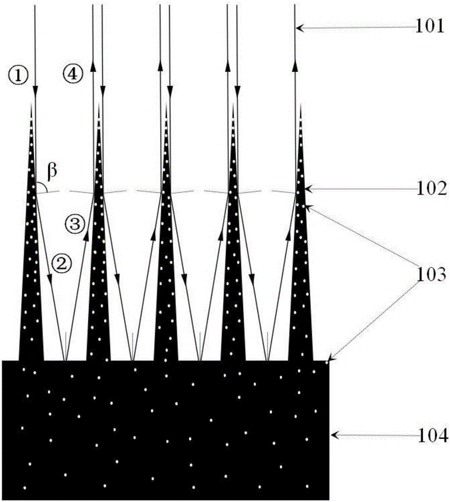
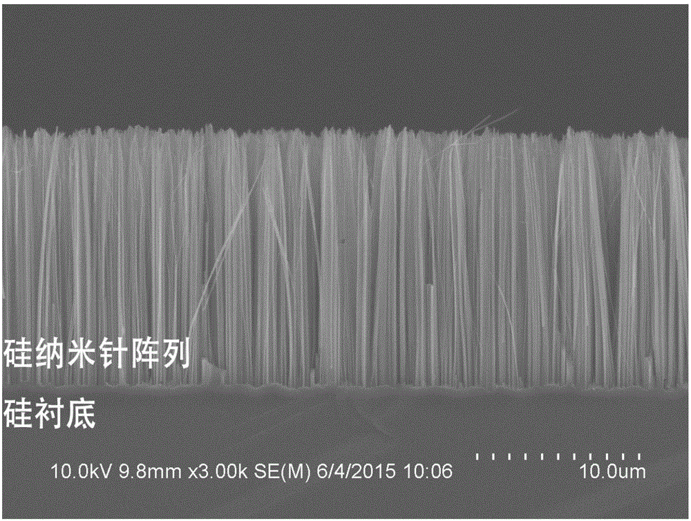
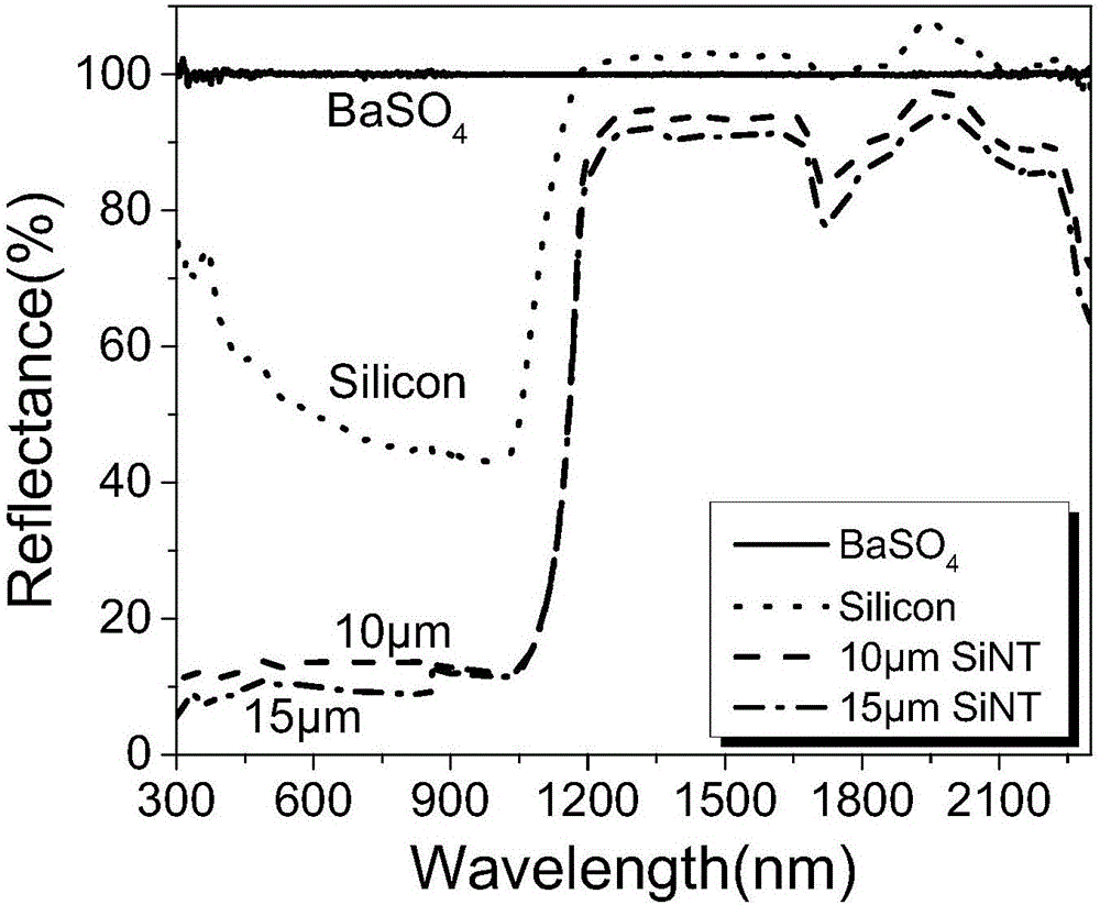
[0024] The silicon nanoneedle-based terahertz wave broadband absorbing material provided in this embodiment has a structure such as figure 1 , figure 2 As shown, it includes silicon nanoneedle array and heavily doped silicon substrate.

[0025] The preparation process of the above absorbing material is described below with an n-type silicon nanoneedle array with a length of 15 μm:

[0026] Step 1: First cut the heavily doped n-type single crystal silicon wafer into a square of 15mm×15mm, then ultrasonically clean it with acetone of appropriate concentration, absolute ethanol and deionized water for 10 minutes, and then use high-pressure nitrogen Blow dry the silicon wafer;

[0027] Step 2: Put the cleaned silicon wafer into the pre-prepared AgNO 3 Soak in HF / HF solution for 60 m...


PUM


Abstract

The invention belongs to the technical field of electromagnetic function materials, and particularly provides a terahertz wave broadband absorbing material based on silicon nanoneedles, which aims at overcoming the defects of narrow absorbing bandwidth, complicated manufacturing technology, poor device stability and high preparation cost of the existing terahertz wave absorbing device. The terahertz wave broadband absorbing material comprises a silicon nanoneedle array and a silicon substrate, wherein the silicon nanoneedle array consists of a plurality of silicon nanoneedles which are uniformly distributed on the silicon substrate; the silicon nanoneedles are vertically arranged at the surface of the silicon susbtrate; the silicon nanoneedle array and the silicon substrate are made of the same material, and respectively adopt n or p type heavily-doped semiconductor silicon, and the resistivity is smaller than or equal to 0.1ohm cm. The terahertz wave broadband absorbing material manufactured by the silicon nanoneedle array structure has the advantages that the structure is simple, and the absorbing rate of terahertz wave reaches 90% within the range of 0.2 to 1.2Thz; by adopting a simple metal-assisted chemical etching method, the preparation technology is simple, and the cost is low.

Description

technical field [0001] The invention belongs to the technical field of electromagnetic functional materials, and relates to an electromagnetic wave absorption structure, in particular to a terahertz wave broadband absorption material based on silicon nano needles. Background technique [0002] Terahertz (THz) waves refer to electromagnetic waves with a frequency ranging from 0.1 THz to 10 THz, between millimeter waves and infrared light, with a wavelength span of 30 μm to 3 mm. This frequency band is the frequency band for the transition from macroelectronics to microelectronics. It has many superior characteristics and shows great application potential in national defense and military, satellite communication, medical diagnosis, etc. Therefore, related research in the field of terahertz has great practical significance to national economy and national security. [0003] Terahertz wave absorbing materials have important application value in terahertz wave energy capture, de...

Claims


Application Information

Patent Timeline
Patent Type & Authority Applications(China)
IPC IPC(8): H01Q17/00
CPCH01Q17/00
Inventor 文岐业史中伟刘浩天陈智文天龙杨青慧张怀武涂翔宇刘洋
Owner UNIV OF ELECTRONICS SCI & TECH OF CHINA
Why Eureka
Try Eureka