Method for removing metal buried layer protrusions and method for preparing air gap

A metal and metal loss technology, which is applied in the fields of electrical components, semiconductor/solid-state device manufacturing, electric solid-state devices, etc., can solve the problems of low physical strength of the air gap, collapse of the air gap, device failure, etc.

Active Publication Date: 2017-06-06
SHANGHAI INTEGRATED CIRCUIT RES & DEV CENT
View PDF3 Cites 0 Cited by
  • Summary
  • Abstract
  • Description
  • Claims
  • Application Information

AI Technical Summary

Problems solved by technology

Buried layer bumps are prone to air gap collapse during the subsequent dielectric film deposition p

Method used


Image

  • Method for removing metal buried layer protrusions and method for preparing air gap
  • Method for removing metal buried layer protrusions and method for preparing air gap
  • Method for removing metal buried layer protrusions and method for preparing air gap

Examples


Embodiment Construction

[0029] In order to make the content of the present invention clearer and easier to understand, the content of the present invention will be further described below in conjunction with the accompanying drawings. Of course, the present invention is not limited to this specific embodiment, and general replacements known to those skilled in the art are also covered within the protection scope of the present invention.

[0030] The following is attached Figure 1-8 The present invention will be described in further detail with specific examples. It should be noted that the drawings are all in a very simplified form, using imprecise scales, and are only used to facilitate and clearly achieve the purpose of assisting in describing the present embodiment.

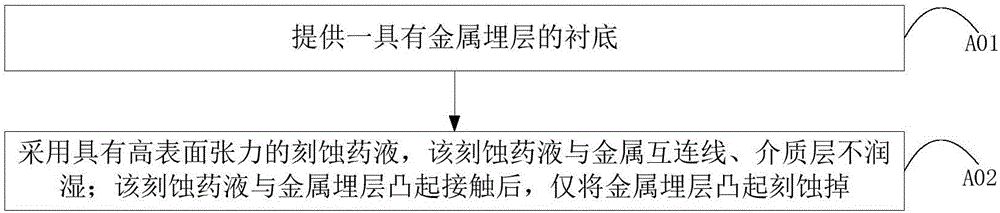
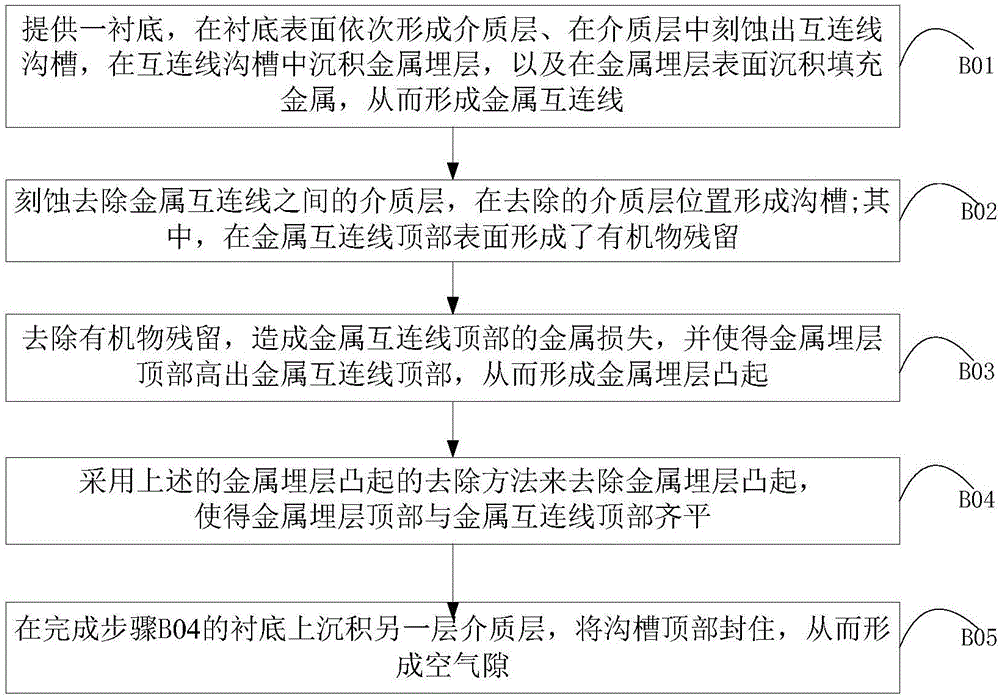
[0031] see figure 1 , a method for removing protrusions of a buried metal layer, comprising;

[0032] Step A01: providing a substrate with a buried metal layer;

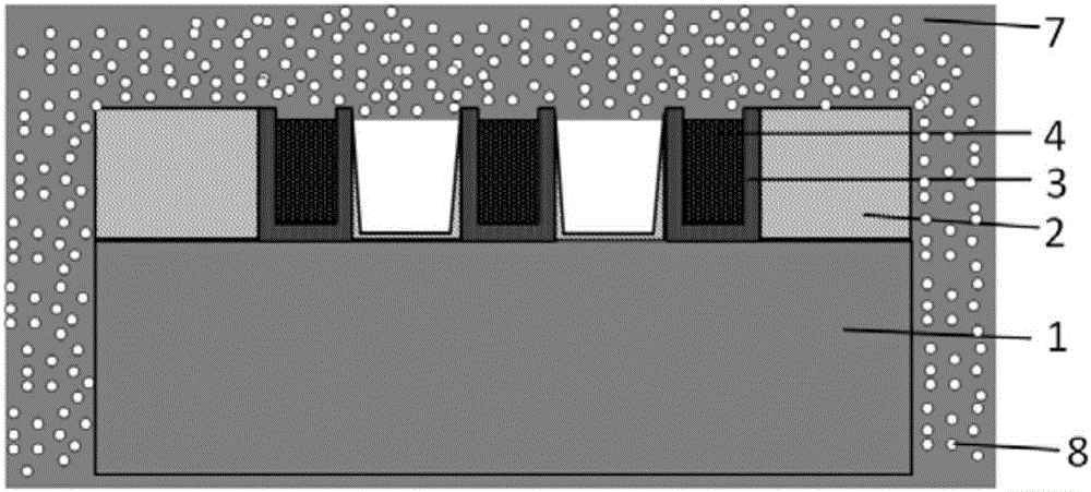
[0033] Specifically, see figure 2 , the substrate 1 can be a m...


PUM


Abstract

The invention provides a method for removing metal buried layer protrusions and a method for preparing an air gap. Wet etching with high surface tension is used for etching the metal buried layer protrusions. In order to avoid excess etching of an etching liquid to a dielectric layer in the air gap structure and a metal buried layer, a method for improving the surface tension of the etching liquid is used so that the etching liquid only remains on a substrate surface including the surface of the metal buried layer and is prevented from entering the a groove where the air gap is to be formed. Thus, the metal buried layer protrusions are successfully removed on the premise that the air gap structure is not damaged, thereby reducing the K value of the dielectric layer.

Description

technical field [0001] The invention relates to the technical field of integrated circuit manufacturing, in particular to a method for removing protrusions of a buried metal layer and a method for preparing air gaps. Background technique [0002] With the continuous development and progress of integrated circuit technology, the critical dimensions of semiconductor manufacturing processes continue to shrink, and the cross-sectional area and distance between interconnections on the chip continue to decrease. The increased interconnection resistance R and parasitic capacitance C greatly increase the time constant RC of the interconnection. Therefore, the time constant RC of the interconnection line accounts for an increasing proportion of the total delay of the integrated circuit, which becomes the main reason for limiting the interconnection speed. Above 0.13um process, semiconductors usually use aluminum as the metal material for subsequent wiring. When entering the process...

Claims


Application Information

Patent Timeline
IPC IPC(8): H01L21/768
CPCH01L21/7682H01L21/7684H01L2221/1042
Inventor 姚嫦娲肖慧敏
Owner SHANGHAI INTEGRATED CIRCUIT RES & DEV CENT
Why Eureka
Try Eureka