A pulsed laser single event effect back-irradiation positioning method

A single-event effect, pulsed laser technology, which is applied in the direction of single semiconductor device testing, instruments, measuring devices, etc., can solve the problem that the position coordinates of the back and front of the die cannot be converted to each other, and cannot fully meet the needs of pulsed laser back irradiation positioning. , can not form back sensitive nodes and other problems, to achieve the effect of saving purchase and transformation costs, reducing experimental costs, and reducing the difficulty of pretreatment and welding

Active Publication Date: 2019-05-03
NORTHWEST INST OF NUCLEAR TECH
View PDF2 Cites 0 Cited by
  • Summary
  • Abstract
  • Description
  • Claims
  • Application Information

AI Technical Summary

Problems solved by technology

Although this method can determine single event effect sensitive nodes from the back side, it cannot complete the mutual conversion of the position coordinates of the back side and the front side of the die, and cannot form a mapping from the back side sensitive nodes to the front side layout.
Also, getting the die out and soldering it to the board is more difficult for commercial devices
Therefore, this method cannot fully meet the needs of pulsed laser back-irradiation positioning, and is more suitable for back-irradiation experiments of self-designed unpackaged chips

Method used


Image

  • A pulsed laser single event effect back-irradiation positioning method
  • A pulsed laser single event effect back-irradiation positioning method
  • A pulsed laser single event effect back-irradiation positioning method

Examples


Embodiment Construction

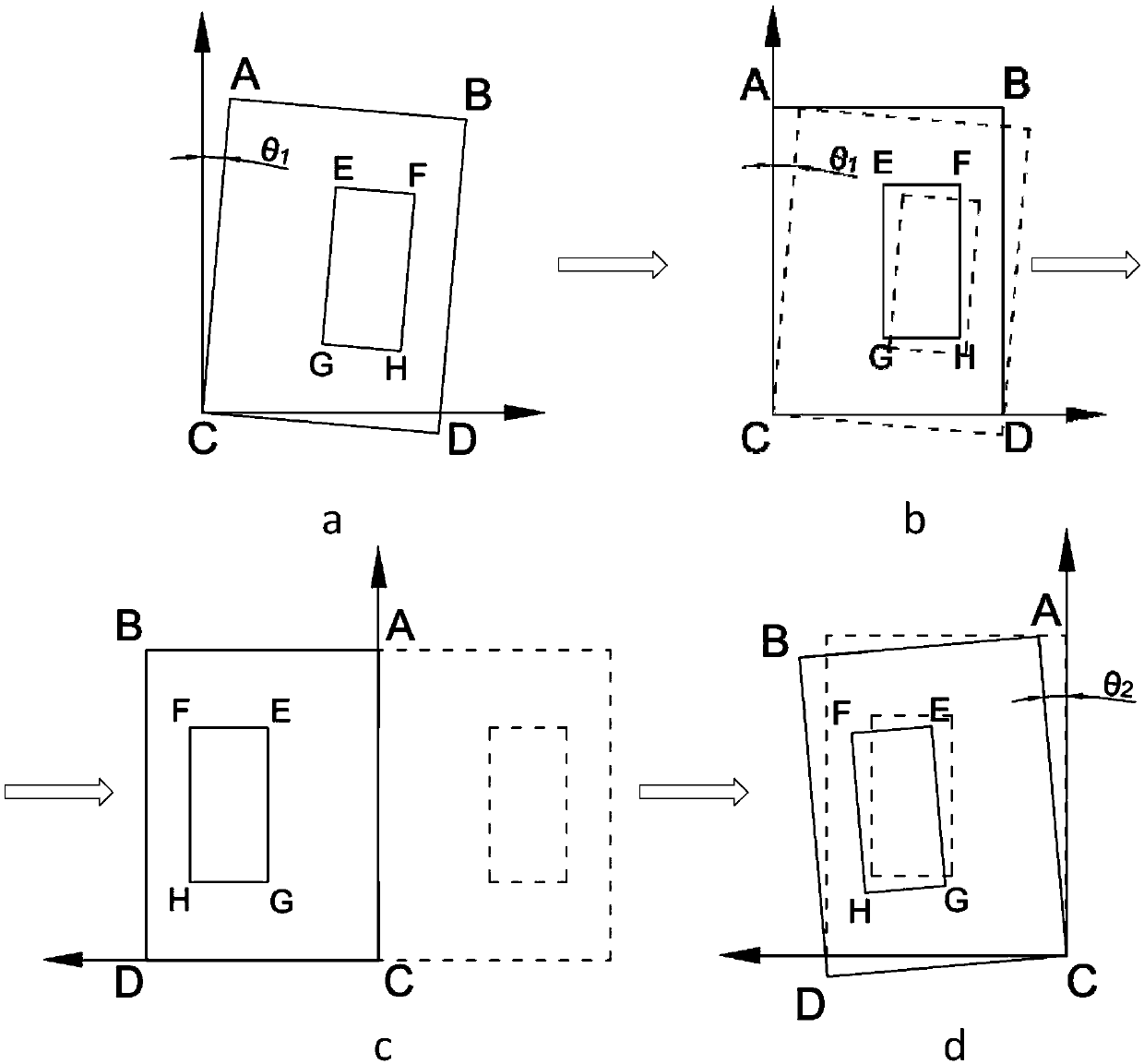
[0030] The present invention will be further described below in conjunction with the accompanying drawings.

[0031] figure 1 The transformation operation steps for the die and the planar view of the area to be tested are given:

[0032] (1) Use the three-dimensional mobile platform control software to obtain the coordinate values ​​of the four vertices A, B, C, and D on the front of the tube core and the four vertices E, F, G, and H of the area to be tested. According to the coordinate values, use AutoCAD to make the tube Core front plan view, as in figure 1 Shown in a.

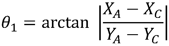
[0033] (2) According to the actual coordinates of A and C obtained in (1), calculate the angle θ between AC and the Y axis 1 , and according to θ 1 Rotate the planar graph to a position orthogonal to the coordinate axes, such as figure 1 Shown in b. Angle θ between AC and Y axis 1 The calculation formula is:

[0034]

[0035] where X A 、X C and Y A , Y C They are the abscissa and ordinate of p...


PUM


Abstract

The invention provides a pulse laser single event effect backside irradiation positioning method comprising the following steps: measuring tube core and to-be-measured area peak coordinates; using mapping software to draw a tube core front side planar graph; rotating the front side planar graph for two times, mirroring the front side planar graph for one time, and translating the front side planar graph for one time, thus obtaining the to-be-measured area position coordinates in backside irradiation. The method can position the to-be-measured area, assigned from the front side, on the chip backside when an infrared imaging system is absent, and can carry out the irradiation test, thus saving purchase and reconstruct cost of a pulse laser backside irradiation optical path system, and reducing the experiment cost.

Description

technical field [0001] The invention relates to a pulse laser single-event effect experimental method of a semiconductor device, in particular to a pulse laser single-event effect back-irradiation positioning method without an infrared imaging system. Background technique [0002] There is a very strong natural radiation environment in the space outside the atmosphere, mainly from cosmic rays, solar particles, the Van Allen radiation belt around the earth, X-rays and electromagnetic radiation, etc. Therefore, the electronic components in the aircraft must consider the total dose Effects of space radiation effects such as TID and single event effects (SEE). With the rapid development of semiconductor technology, the integration of electronic devices used in spacecraft continues to increase, the feature size of devices is getting smaller and smaller, the operating voltage is getting lower and lower, the corresponding critical charge is getting smaller and smaller, and the infl...

Claims


Application Information

Patent Timeline
Patent Type & Authority Patents(China)
IPC IPC(8): G01B21/00G01R31/26G01R31/265
CPCG01B21/04G01R31/2644G01R31/2656
Inventor 郭红霞魏佳男张凤祁罗尹虹丁李利张阳潘霄宇刘玉辉
Owner NORTHWEST INST OF NUCLEAR TECH
Why Eureka
Try Eureka