
Three-valued sensitive amplifier and SRAM array implementing same

一种灵敏放大器、阵列的技术,应用在灵敏放大器领域,能够解决延时大、漏电流和极间电容大、芯片成品率低等问题,达到功耗降低、工作速度提高的效果

Active Publication Date: 2017-06-09
NINGBO UNIV
View PDF4 Cites 4 Cited by
  • Summary
  • Abstract
  • Description
  • Claims
  • Application Information

AI Technical Summary

Problems solved by technology

[0003] The process size has entered the nanometer level, the threshold voltage mismatch of MOS transistors is becoming more and more serious, the offset voltage of the three-valued sensitive amplifier designed with CMOS technology is getting larger and larger, and the chip yield is low
The physical characteristics of the MOS tube determine its large leakage current and inter-electrode capacitance, and the designed three-valued sense amplifier has high power consumption and large delay

Method used


Image

  • Three-valued sensitive amplifier and SRAM array implementing same
  • Three-valued sensitive amplifier and SRAM array implementing same
  • Three-valued sensitive amplifier and SRAM array implementing same

Examples


Embodiment

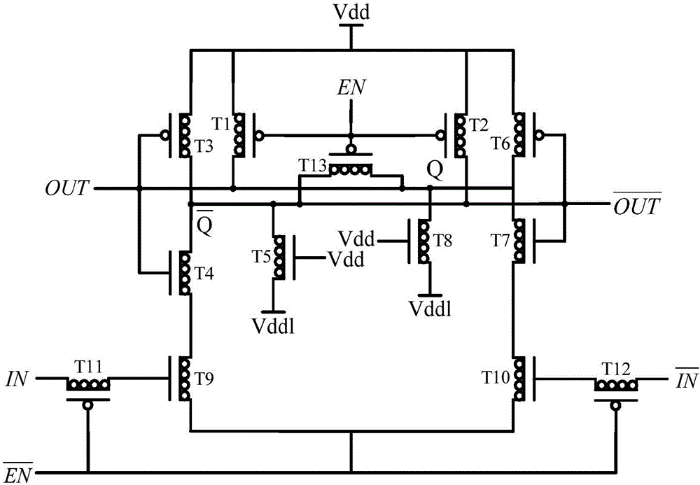
[0021] Example: such as figure 1As shown, a three-valued sensitive amplifier includes a first CNFET tube T1, a second CNFET tube T2, a third CNFET tube T3, a fourth CNFET tube T4, a fifth CNFET tube T5, a sixth CNFET tube T6, and a seventh CNFET tube Tube T7, eighth CNFET tube T8, ninth CNFET tube T9, tenth CNFET tube T10, eleventh CNFET tube T11, twelfth CNFET tube T12 and thirteenth CNFET tube T13; first CNFET tube T1, second The CNFET tube T2, the third CNFET tube T3, the sixth CNFET tube T6, the eleventh CNFET tube T11, the twelfth CNFET tube T12 and the thirteenth CNFET tube T13 are all P-type CNFET tubes, the fourth CNFET tube T4, the The fifth CNFET tube T5, the seventh CNFET tube T7, the eighth CNFET tube T8, the ninth CNFET tube T9 and the tenth CNFET tube T10 are all N-type CNFET tubes; the source of the first CNFET tube T1 and the source of the second CNFET tube T2 The source, the source of the third CNFET transistor T3, the gate of the fifth CNFET transistor T5, t...

Embodiment 1

[0035] Embodiment one: if figure 1 and Figure 5As shown, a SRAM array implemented by a three-value sense amplifier, including a three-value sense amplifier, a three-value storage array, a first inverter G1, a second inverter G2, a third inverter G3, and a fourth inverter device G4, the fourteenth CNFET tube T14, the fifteenth CNFET tube T15, the sixteenth CNFET tube T16, the seventeenth CNFET tube T17, the eighteenth CNFET tube T18, and the nineteenth CNFET tube T19; the memory array has a bit line and anti-phase line, the fourteenth CNFET tube T14, the fifteenth CNFET tube T15, the sixteenth CNFET tube T16 and the eighteenth CNFET tube T18 are all P-type CNFET tubes, the seventeenth CNFET tube T17 and the nineteenth CNFET tube T17 The CNFET tubes T19 are all N-type CNFET tubes; the three-valued sensitive amplifier includes the first CNFET tube T1, the second CNFET tube T2, the third CNFET tube T3, the fourth CNFET tube T4, the fifth CNFET tube T5, and the sixth CNFET tube T...

Embodiment 2

[0036] Embodiment two: if figure 1 and Figure 5 As shown, a SRAM array implemented by a three-value sense amplifier, including a three-value sense amplifier, a three-value storage array, a first inverter G1, a second inverter G2, a third inverter G3, and a fourth inverter device G4, the fourteenth CNFET tube T14, the fifteenth CNFET tube T15, the sixteenth CNFET tube T16, the seventeenth CNFET tube T17, the eighteenth CNFET tube T18, and the nineteenth CNFET tube T19; the memory array has a bit line and anti-phase line, the fourteenth CNFET tube T14, the fifteenth CNFET tube T15, the sixteenth CNFET tube T16 and the eighteenth CNFET tube T18 are all P-type CNFET tubes, the seventeenth CNFET tube T17 and the nineteenth CNFET tube T17 The CNFET tubes T19 are all N-type CNFET tubes; the three-valued sensitive amplifier includes the first CNFET tube T1, the second CNFET tube T2, the third CNFET tube T3, the fourth CNFET tube T4, the fifth CNFET tube T5, and the sixth CNFET tube ...


PUM


Abstract

The invention discloses a three-valued sensitive amplifier and an SRAM array implementing the same. The three-valued sensitive amplifier comprises a first CNFET tube, a second CNFET tube, a third CNFET tube, a fourth CNFET tube, a fifth CNFET tube, a sixth CNFET tube, a seventh CNFET tube, an eighth CNFET tube, a ninth CNFET tube, a tenth CNFET tube, an eleventh CNFET tube, a twelfth CNFET tube and a thirteenth CNFET tube. The SRAM array comprises the three-valued sensitive amplifier, a three-valued memory array, a first phase inverter, a second phase inverter, a third phase inverter, a fourth phase inverter, a fourteenth CNFET tube, a fifteenth CNFET tube, a sixteenth CNFET tube, a seventeenth CNFET tube, an eighteenth CNFET tube and a nineteenth CNFET tube. The three-valued sensitive amplifier disclosed by the invention has the advantages of being relatively low in power consumption, relatively short in delayed time and relatively high in rate of chip finished products.

Description

technical field [0001] The invention relates to a sensitive amplifier, in particular to a three-valued sensitive amplifier and an SRAM array realized therefor. Background technique [0002] With the development of integrated circuits, more than 50% of transistors in microprocessors are used in memory design. The design of the memory has a great influence on the performance of the microprocessor, so the design of the high-performance memory is particularly important. Improving the performance of the peripheral circuits of the memory can improve the performance of the memory. The sense amplifier is one of the important peripheral circuits of the memory, and the performance of the sense amplifier directly affects the speed of the memory and its power consumption. The document "Lin S, Kim Y B, Lombardi F. Design of a Ternary Memory Cell Using CNTFETs [J]. IEEE Transactions on Nanotechnology, 2012, 11(5): 1019-1025." proposed a three-value SRAM cell (three-value static random s...

Claims


Application Information

Patent Timeline
Patent Type & Authority Applications(China)
IPC IPC(8): G11C7/06G11C11/417H10K99/00
CPCG11C7/062G11C11/417G11C7/065G11C11/419G11C11/412H10K19/10H10K85/221H10K10/484
Inventor 汪鹏君龚道辉康耀鹏张会红
Owner NINGBO UNIV
Learn More