A method for increasing the via slope angle of the via layer
A technology of slope angle and via hole, which is applied in the direction of electrical components, circuits, semiconductor/solid-state device manufacturing, etc., to achieve the effects of reducing key dimension distortion, improving circuit quality, and good lapping effect
- Summary
- Abstract
- Description
- Claims
- Application Information
AI Technical Summary
Problems solved by technology
Method used
Image
Examples
Embodiment Construction
[0020] The following will clearly and completely describe the technical solutions in the embodiments of the present invention with reference to the drawings in the embodiments of the present invention. The values of the following components are only preferred embodiments, and do not constitute limitations on the scope of protection of the present invention.
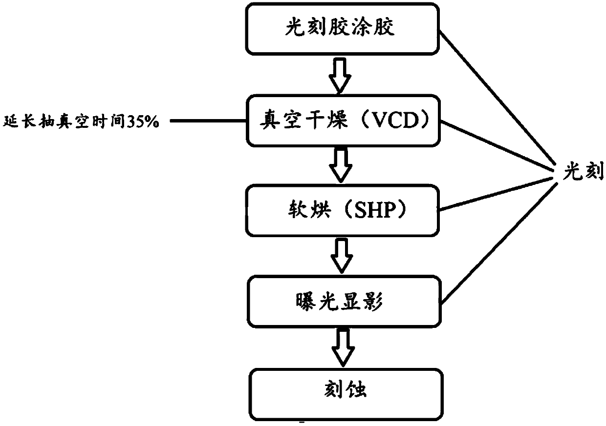
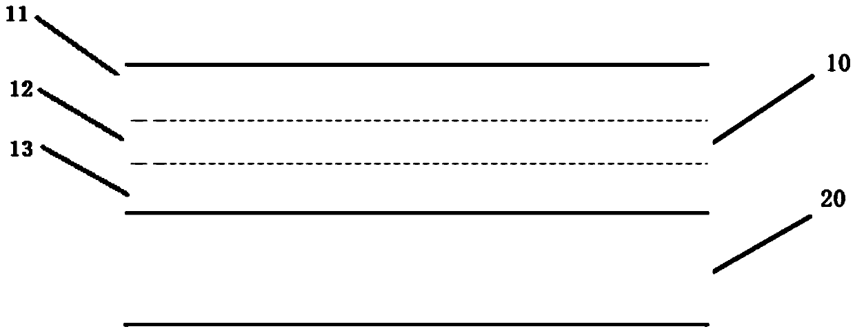
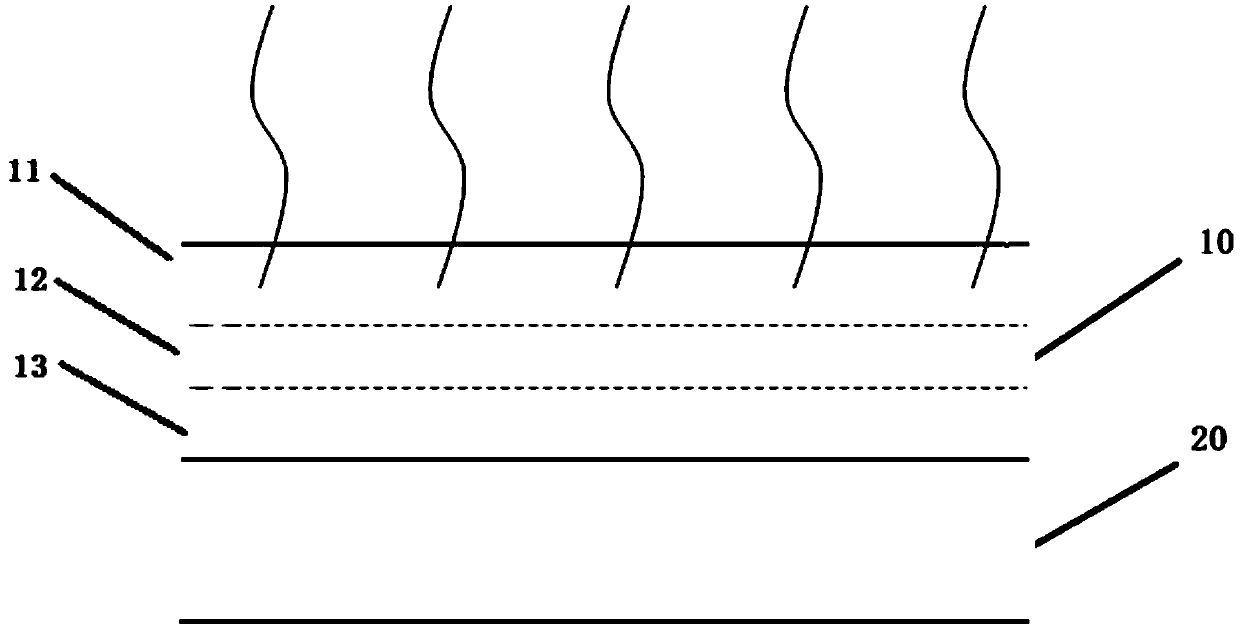
[0021] see figure 1 , is a fabrication flowchart of a method for increasing the via hole slope angle of the via layer provided by an embodiment of the present invention. In this embodiment, the method for increasing the via hole slope angle of the via layer includes a photolithography step and an etching step, and the photolithography step includes a photoresist coating step and a vacuum drying (VCD) step , soft baking (SHP) step, exposure and development step; In the photoresist coating step, the photoresist 10 is coated on the film layer 20, as figure 2 , is a schematic structural view of the via layer (the substra...
PUM
 Abstract
Description
Claims
Application Information


