Semi-reflecting and semi-transmitting glass with electromagnetic shielding function
A semi-reflective, semi-transparent and electromagnetic shielding technology, applied in the coating and other directions, can solve the problems that conductive materials cannot be effectively protected, increase the process and cost, and reduce the shielding effect, so as to achieve excellent reliability, reduce production costs and reliability. high effect
- Summary
- Abstract
- Description
- Claims
- Application Information
AI Technical Summary
Problems solved by technology
Method used
Image


Examples
Embodiment 1
[0022] Example 1: The three-layer common film-based semi-reflective and semi-transparent structure is: substrate / H1 / L / H, where H represents a high refractive index material. In this example, the substrate is selected as transparent substrate glass, and the H layer is Nb 2 O 5 , the refractive index is 2.5, and the film thickness of the top H layer is 50 nm; L represents a low refractive index material, in this example, SiO is selected 2 , the refractive index is 1.46, and the film thickness is 80 nm. The H1 layer is ITO, the refractive index is 2.1, the film thickness is 60 nm, and the sheet resistance is 30 ohms. The test reflectivity from the air surface (non-film surface) of the substrate is 50%, and the reflection is blue-green. In the uniform chromaticity space (L, a, b), L=73, a=-10, b=-22.
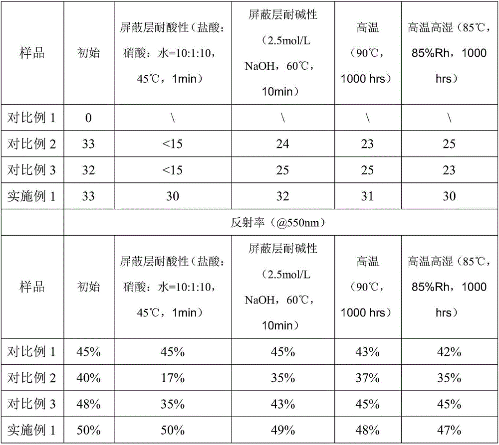
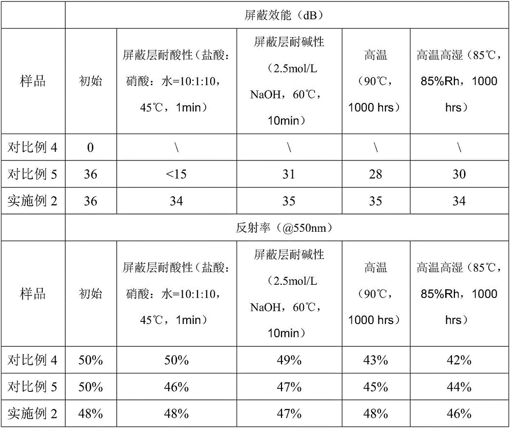
[0023] Compared with Example 1, the shielding effectiveness and reflectivity of Comparative Examples 1-3 are shown in Table 1 below:
[0024] Table 1
[0025]
[0026]
[00...
Embodiment 2
[0030] Example 2: The five-layer ordinary film-based semi-reflective and semi-transparent structure is: substrate / H1 / L / H / L / H, where H represents a high refractive index material. In this example, the substrate is selected as transparent substrate glass, and the H layer is Nb 2 O 5 , the refractive index is 2.5, the film thickness of the bottom H layer is 33 nm, and the film thickness of the top H layer is 65 nm; L represents a low refractive index material, in this example, SiO is selected 2 , the refractive index is 1.46, the film thickness of the bottom L layer is 2 nm, and the film thickness of the upper L layer is 90 nm. The H1 layer on the other side of the substrate is ITO, the refractive index is 2.1, the film thickness is 95 nm, and the sheet resistance is 17 ohms. The test reflectivity from the air surface (non-film surface) of the substrate is 48%, and the reflected color is almost colorless. In the uniform chromaticity space (L, a, b), L=75, a=0, b=-1.
[0031] Co...
PUM
| Property | Measurement | Unit |
|---|---|---|
| Film thickness | aaaaa | aaaaa |
| Film thickness | aaaaa | aaaaa |
| Resistance | aaaaa | aaaaa |
Abstract
Description
Claims
Application Information
 - R&D
- Intellectual Property
- Life Sciences
- Materials
- Tech Scout
- Unparalleled Data Quality
- Higher Quality Content
- 60% Fewer Hallucinations
Browse by: Latest US Patents, China's latest patents, Technical Efficacy Thesaurus, Application Domain, Technology Topic, Popular Technical Reports.
© 2025 PatSnap. All rights reserved.Legal|Privacy policy|Modern Slavery Act Transparency Statement|Sitemap|About US| Contact US: help@patsnap.com