Optical film material, method for preparing same, display substrate and display device

An optical film and display substrate technology, applied in optics, optical components, optical components, etc., can solve the problem of small viewing angle, only see all black or white, can not see color, etc., to maintain brightness, expand The effect of the angle range

Pending Publication Date: 2017-06-13
BOE TECH GRP CO LTD +1
View PDF6 Cites 15 Cited by
  • Summary
  • Abstract
  • Description
  • Claims
  • Application Information

AI Technical Summary

Problems solved by technology

[0002] The problem with TFT-LCD produced by the traditional process is that when the backlight is output through polarizers, thin film transistors (TFT), etc., the output light has directionality, that is to say, most of the light comes from the screen. Therefore, when the LCD is viewed from a larger angle, the original color cannot be seen, or even all black or all white can be seen.
In particular, the TN mode TFT-LCD display has a smaller viewing angle due to the rotation of the liquid crystal. When the viewing angle increases, the picture display quality is seriously degraded.

Method used


Image

  • Optical film material, method for preparing same, display substrate and display device
  • Optical film material, method for preparing same, display substrate and display device
  • Optical film material, method for preparing same, display substrate and display device

Examples


Embodiment 1

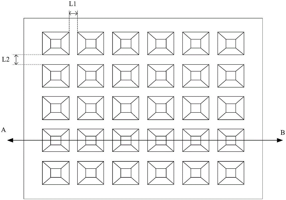
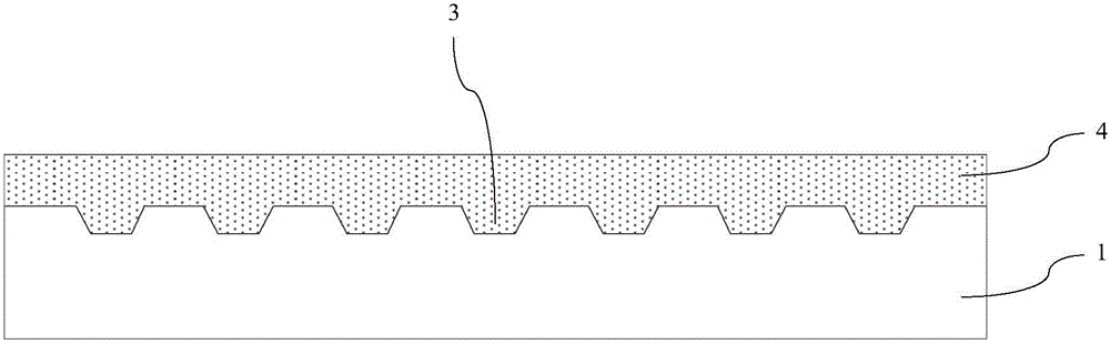
[0035] Such as figure 1 and 2 As shown, this embodiment provides an optical film material, which includes: a substrate 1 and a planarization layer 4; a groove 3 is provided on the substrate 1, and the cross-sectional area of ​​the groove 3 is parallel to the plane where its bottom surface is located, along the The direction away from the bottom surface gradually increases; the planarization layer 4 is located on the side of the substrate 1 with the groove 3 , and the refractive index of the planarization layer 4 is greater than that of the substrate 1 . The planarization layer 4 at least fills up the groove 3 , and the surface of the planarization layer 4 is flat.

[0036] Specifically, the optical film material in this embodiment can be applied to a display substrate, and the display substrate can be boxed with an array substrate to form a display panel, and the optical film material is located on the light-emitting surface side of the display panel; the display substrate ca...

Embodiment 2

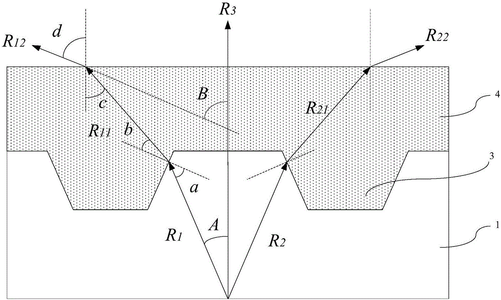
[0045] Such as Figure 5As shown, this embodiment provides a method for preparing an optical film, and the display substrate may be the optical film in Embodiment 1. The preparation method includes: etching the substrate 1 to form a groove 3, and the angle between the side surface and the bottom surface of the groove 3 is an acute angle; forming a planarization layer on the substrate 1 on which the groove 3 is formed. 4.

[0046] The steps for preparing the optical film are described in detail below.

[0047] Step 1: Coating a photoresist 2 on the substrate 1, exposing and developing to form a photoresist reserved area 21 and a photoresist unreserved area.

[0048] Step 2: Etching the non-retained photoresist area using plasma etching equipment to form the groove 3 .

[0049] This step specifically includes: using ICP plasma etching equipment, using Ar and CHF 3 The mixed gas is an etching gas to etch the substrate 1, specifically, the Ar inert gas is ionized into Ar in th...

Embodiment 3

[0054] This embodiment provides a display device, which includes the display substrate in Embodiment 1. Therefore, the display device of this embodiment has a wider viewing angle and better display effect.

[0055] Wherein, the display device can be a liquid crystal display device or an electroluminescent display device, such as a liquid crystal panel, an electronic paper, an OLED panel, a mobile phone, a tablet computer, a TV set, a monitor, a notebook computer, a digital photo frame, a navigator, etc. product or part. Figure 6 Shown in is a liquid crystal display device, which includes an array substrate and a color filter substrate, and a liquid crystal layer 7 arranged between the array substrate and the color filter substrate, wherein the display substrate in Embodiment 1 is also Figure 6 The color filter substrate specifically includes a base 1 with grooves 3 , a planarization layer 4 , a color filter layer 9 , and an alignment layer 8 ; the array substrate includes a...


PUM

PropertyMeasurementUnit
depthaaaaaaaaaa
depthaaaaaaaaaa
thicknessaaaaaaaaaa

Abstract

The invention provides an optical film material, a method for preparing the same, a display substrate and a display device, and belongs to the field of display technologies. The optical film material comprises a base and a flattened layer. Grooves are formed in the base, are parallel to the cross section of a plane where the bottom surface of the base and are gradually enlarged along the direction which is far away from the bottom surface; the flattened layer is positioned on the side, where the grooves are formed, of the base, and the refractive index of the flattened layer is higher than the refractive index of the base. The optical film material, the method, the display substrate and the display device have the advantages that incident light can be refracted by the side surfaces of the grooves when the optical film material is applied to the display substrate, and accordingly emergence angle ranges of light rays can be extended; particularly, incident light beams which are perpendicular to the bottoms of the grooves or are perpendicular to horizontal planes between the grooves cannot be refracted when transmitted through interfaces, and accordingly the brightness of light under forward visual angles can be kept.

Description

technical field [0001] The invention belongs to the field of display technology, and in particular relates to an optical film material and a preparation method thereof, a display substrate, and a display device. Background technique [0002] The problem with TFT-LCD produced by the traditional process is that when the backlight is output through polarizers, thin film transistors (TFT), etc., the output light has directionality, that is to say, most of the light comes from the screen. Therefore, when the LCD is viewed from a larger angle, the original color cannot be seen, and even only black or white can be seen. Especially the TN mode TFT-LCD display has a smaller viewing angle due to the rotation mode of the liquid crystal. When the viewing angle increases, the display quality of the picture is seriously degraded. With people's pursuit of display picture quality, the requirements for TFT-LCD are getting higher and higher. Therefore, how to increase the viewing angle of TF...

Claims


Application Information

Patent Timeline
Patent Type & Authority Applications(China)
IPC IPC(8): G02F1/1335G02F1/1333
CPCG02F1/133504G02F1/133357B29D11/00278B29D11/00788G02F2202/16G02F1/133331G02F1/133562B32B3/30B32B33/00B32B2255/20B32B2307/418B32B2457/20C23C14/086C23C14/35G02B27/0081G03F7/0005
Inventor 段献学宫奎
Owner BOE TECH GRP CO LTD
Why Eureka
Try Eureka