All-CMOS (Complementary Metal Oxide Semiconductor) based reference voltage source with high power supply rejection ratio

A high power supply rejection ratio, reference voltage source technology, applied in the direction of adjusting electrical variables, control/regulation systems, instruments, etc., can solve the problems of large reference voltage source layout area, low power supply suppression, high power consumption, etc., to achieve low power consumption , low power supply voltage adjustment rate, and the effect of reducing production costs

Active Publication Date: 2017-06-13
GUILIN UNIV OF ELECTRONIC TECH
View PDF5 Cites 16 Cited by
  • Summary
  • Abstract
  • Description
  • Claims
  • Application Information

AI Technical Summary

Problems solved by technology

[0004] The technical problem to be solved by the present invention is that the existing reference voltage source has a large layout area, high power consumption, and relatively low power supply rejection, and provides a high power supply rejection ratio full CMOS reference voltage source

Method used


Image

  • All-CMOS (Complementary Metal Oxide Semiconductor) based reference voltage source with high power supply rejection ratio
  • All-CMOS (Complementary Metal Oxide Semiconductor) based reference voltage source with high power supply rejection ratio
  • All-CMOS (Complementary Metal Oxide Semiconductor) based reference voltage source with high power supply rejection ratio

Examples


Embodiment Construction

[0016] Below in conjunction with accompanying drawing and embodiment, describe technical solution of the present invention in detail:

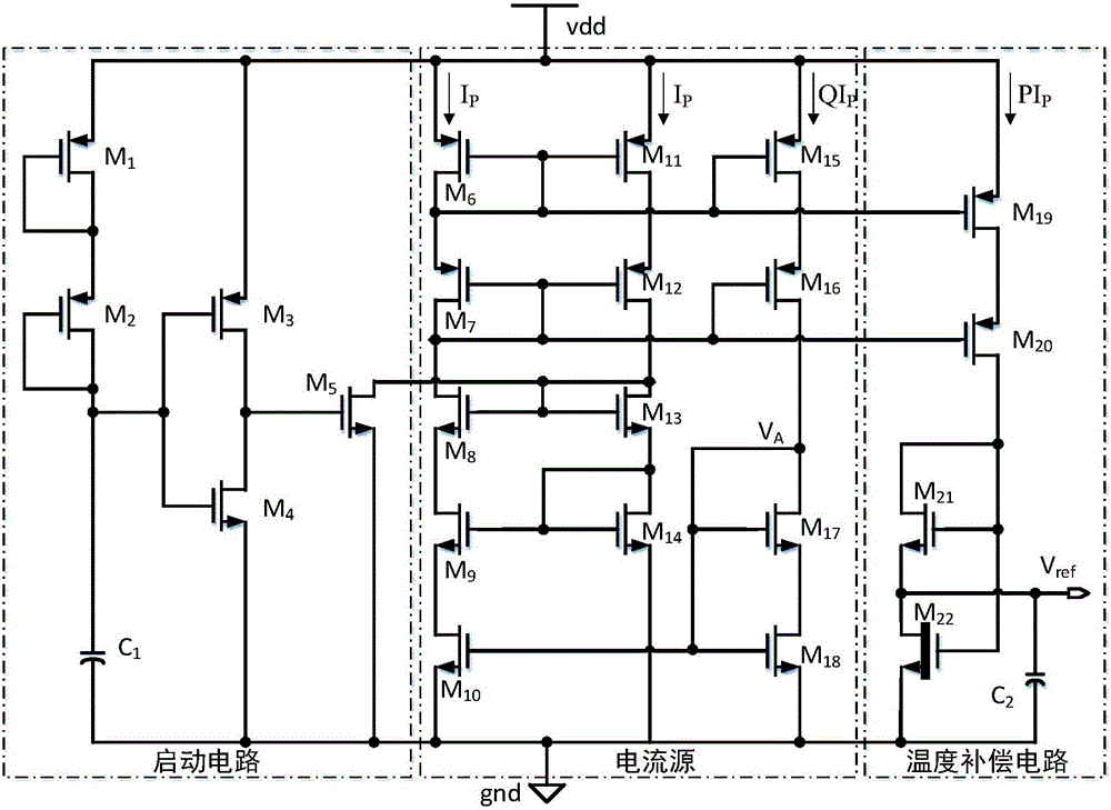
[0017] A high power supply rejection ratio full CMOS voltage reference, such as figure 1 Shown, including start-up circuit, current source and temperature compensation circuit. The output terminal of the start-up circuit is connected to the input terminal of the current source circuit, the output terminal of the current source circuit is connected to the input terminal of the temperature compensation circuit, and the output terminal of the temperature compensation circuit forms the output terminal V of the entire reference voltage source. ref .

[0018] The start-up circuit provides current when the reference voltage source is turned on, so that the reference voltage source gets rid of the degenerate bias point and enters a normal working state. In a preferred embodiment of the present invention, the above startup circuit includes a PMOS tra...


PUM


Abstract

The invention discloses an all-CMOS (Complementary Metal Oxide Semiconductor) reference voltage source with a high power supply rejection ratio, which comprises a reference voltage source. The reference voltage source comprises a starting circuit, a current source circuit and a temperature compensating circuit, wherein an output end of the starting circuit is connected with an input end of the current source circuit; an output end of the current source circuit is connected with an input end of the temperature compensating circuit; an output end of the temperature compensating circuit forms an output end of the whole reference voltage source. The working characteristic of an MOS transistor working in a sub-threshold region is utilized by the all-CMOS reference voltage source, a nanoampere-magnitude reference current is generated; power supply noise is rejected by adopting a cascode current mirror. In addition, the all-CMOS reference voltage source not only has the advantages that the chip area is small and the power consumption is low and is only nanowatt-magnitude, but also has the advantages that the all-CMOS reference voltage source has the high power supply rejection ratio, the temperature drift coefficient is low, and the line-voltage regulation is low; moreover, a resistor, a diode and a triode are not used; the all-CMOS reference voltage source is compatible with a standard CMOS process; the layout area is effectively reduced; the production cost is decreased.

Description

technical field [0001] The invention relates to the technical field of integrated circuits, in particular to a full CMOS reference voltage source with high power supply rejection ratio. Background technique [0002] The reference voltage source is an important module in digital-analog hybrid circuits and analog hybrid circuits, and is often used in voltage management chips, digital-to-analog converters (DAC), analog-to-digital converters (ADC) and phase-locked loops (PLL), In circuits such as low-dropout linear regulators (LDOs), the voltage reference provides a DC reference voltage for the system. A high-precision, high-stability reference voltage source is a necessary unit for high-performance analog integrated circuits. In view of the advantages of low temperature coefficient, high power supply rejection ratio, and compatibility with standard CMOS processes, the CMOS reference voltage source circuit has been widely studied and applied. It provides a system that is affect...

Claims


Application Information

Patent Timeline
Patent Type & Authority Applications(China)
IPC IPC(8): G05F1/567
CPCG05F1/567
Inventor 岳宏卫龚全熙朱智勇徐卫林吴超飞孙晓菲汤寒雪邓进丽
Owner GUILIN UNIV OF ELECTRONIC TECH
Why Eureka
Try Eureka