MMW SMMW silicon-based on-chip end-on-fire antenna

A submillimeter-wave, end-fired antenna technology, applied in the direction of antenna, antenna support/mounting device, antenna grounding switch structure connection, etc., can solve the problems of low gain, reduced radiation efficiency, low resistivity, etc., and achieve simple structure, High efficiency, small size effect

Inactive Publication Date: 2017-06-13
成都中宇微芯科技有限公司
View PDF4 Cites 11 Cited by
  • Summary
  • Abstract
  • Description
  • Claims
  • Application Information

AI Technical Summary

Problems solved by technology

[0003] However, in the existing low-cost silicon-based semiconductor process, the substrate generally has a low resistivity (usually 10Ω.cm), and the energy radiated by the antenna to the space is more through the low-resistance path of the substrate, resulting in gain decline
At the same time, the substrate usually has a high dielectric constant (εr=11.9), which causes the radiation power of the antenna to be confined inside the substrate instead of being radiated to free space, further reducing the radiation efficiency
[0004] Moreover, the on-chip antenna is limited by the radiation area and radiation efficiency, and its gain is often at a very low level (usually less than 0dB), which cannot meet the requirements for high antenna gain.
Moreover, due to the size of the antenna and the front-end circuit, the antenna cannot be used in the case of a large-scale two-dimensional array
[0005] At the same time, in the chip splitting process, due to the influence of the chip cutting process, edge chipping is prone to occur, resulting in chip damage and on-chip antenna performance degradation

Method used


Image

  • MMW SMMW silicon-based on-chip end-on-fire antenna
  • MMW SMMW silicon-based on-chip end-on-fire antenna
  • MMW SMMW silicon-based on-chip end-on-fire antenna

Examples


Embodiment

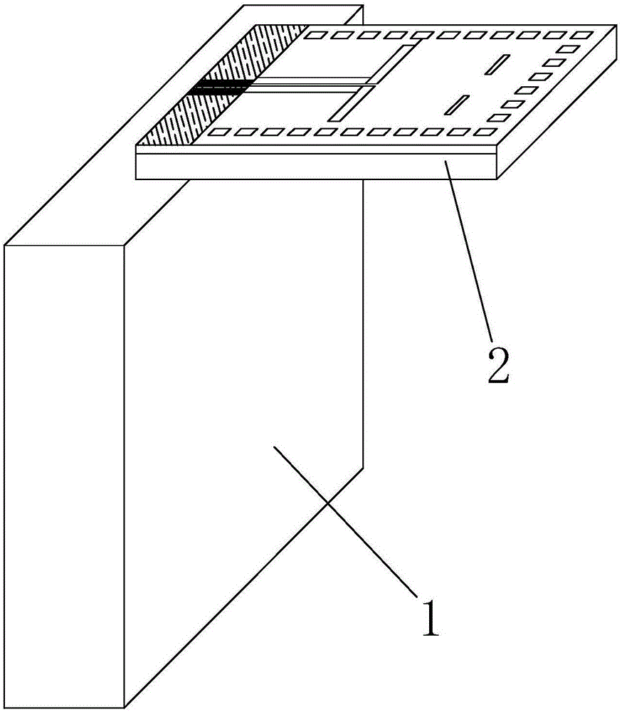
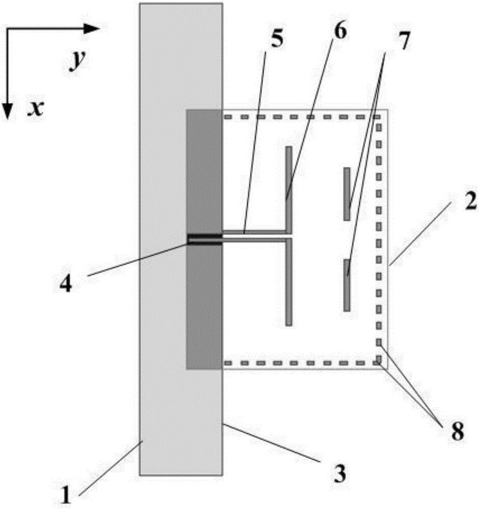
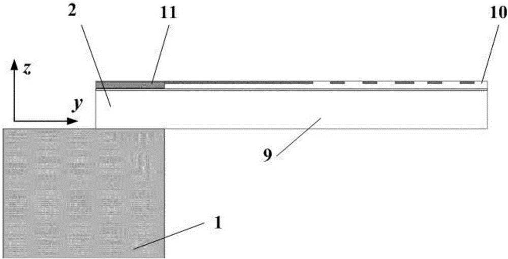
[0027] Such as Figure 1~4 As shown, a millimeter-wave and sub-millimeter-wave silicon substrate-mounted end-fire antenna includes a metal support platform 1, and an on-chip antenna 2 arranged on one side of the metal support platform; the on-chip antenna includes a silicon substrate 9, set SiO on the upper surface of silicon substrate 2 layer 10, and is arranged on the upper surface of the silicon substrate and is located in the SiO 2 The metal wiring layer 11 on one side of the layer; the metal wiring layer is located on the side of the on-chip antenna close to the metal support platform; the metal wiring layer is provided with a CPW feed port 4; the SiO 2 The layer is provided with a parallel double wire 5 connected to the CPW feed port, and is provided with a Yagi antenna active vibrator 6 connected with the parallel double wire; the side of the metal support table close to the on-chip antenna is provided with a reflective surface 3 , the reflector is combined with the g...


PUM


Abstract

The invention discloses an MMW (millimeter Wave) SMMW (Sub Millimeter wave) silicon-based on-chip end-on-fire antenna. The antenna includes a metal support table and an on-chip antenna arranged on one side of the metal support table. The on-chip antenna includes a silicon substrate, a SiO2 layer arranged on the upper surface of the silicon substrate and a metal wiring layer arranged on the upper surface of the upper silicon substrate and one side of the SiO2 layer. The metal wiring layer is disposed on one side, adjacent to the metal support table, of the on-chip antenna. The metal wiring layer is provided with a CPW feed port. The SiO2 layer is provided with parallel double lines connected with the CPW feed port and is provided with a yagi antenna active vibrator connected with the parallel double line. One side face, adjacent to the on-chip antenna, of the metal support table is provided with a reflecting face. The reflecting face and a grounding face of the CPW feed port are combined into a transmitter. The antenna provided by the invention has advantages of simple structure, small size, high efficiency, high gain and engineering convenience and meets application requirements in fields of MMW, SMMW imaging, communication and phase control array and the like.

Description

technical field [0001] The invention relates to a chip-mounted antenna, in particular to a millimeter-wave submillimeter-wave silicon substrate-mounted end-fire antenna. Background technique [0002] The antenna, as the first element at the receiving end and the last element at the transmitting end, must be connected to the circuit, so impedance matching is essential to ensure maximum power transfer. Also, since the antennas are implemented on regular PCBs, gold wire bonds are used to connect them to the IC, which can greatly affect matching, especially at mmWave frequencies, as these bond wires are often non-deterministic and cannot be guaranteed to be repeatable sex. In contrast, the on-chip antenna can be integrated with the front-end circuit at one time, which alleviates the above problems. [0003] However, in the existing low-cost silicon-based semiconductor process, the substrate generally has a low resistivity (usually 10Ω.cm), and the energy radiated by the antenn...

Claims


Application Information

Patent Timeline
Patent Type & Authority Applications(China)
IPC IPC(8): H01Q1/38H01Q1/50H01Q19/30H01Q19/10H01Q1/22
Inventor 邓小东熊永忠王勇李一虎
Owner 成都中宇微芯科技有限公司
Why Eureka
Try Eureka