
PCB soldering flake pulse hot press

A technology for PCB circuit boards and heat presses, which is applied to printed circuits, printed circuit manufacturing, and printed circuit assembly of electrical components, etc. It can solve problems such as loose joints, unevenness, and influence on the welding of electronic components, and achieves easy operation. , simple structure, and the effect of improving welding yield

Pending Publication Date: 2017-06-13
东莞市仪锐电子有限公司
View PDF4 Cites 3 Cited by
  • Summary
  • Abstract
  • Description
  • Claims
  • Application Information

AI Technical Summary

Problems solved by technology

The solder tabs or pads of the PCB circuit board are exposed and used for soldering electronic components. However, in the current low-end PCB circuit boards, the solder tabs or pads often have problems of unevenness and loose bonding, which often affect Soldering to electronic components

Method used


Image

  • PCB soldering flake pulse hot press

Examples


Embodiment Construction

[0015] The structural principle and working principle of the present invention will be further described in detail below in conjunction with the accompanying drawings.

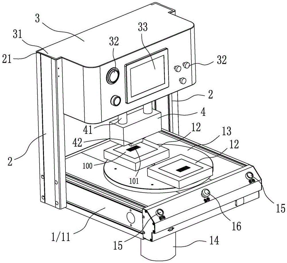
[0016] Such as figure 1 As shown, the present invention is a pulse heat press for PCB circuit board solder tabs, including a machine base 1, two stand 2, a machine head 3 and a heat pressing head 4; the machine base 1 is provided with an operating platform 11 , the middle part above the operating platform 11 is equipped with a circuit board tray 12 for placing the PCB circuit board 100; Machine head 3; described hot pressing head 4 is installed on the lower end of described machine head 3, and the lower end of hot pressing head 4 is corresponding to described circuit board tray 12; Described machine head 3 is provided with a cylinder (in the figure not shown), the telescopic rod of the cylinder is connected to the thermal head 4 to drive the thermal head 4 to press down or rise in a pulsed manner; the thermal...


PUM


Abstract

The invention discloses a PCB soldering flake pulse hot pressing machine. The PCB soldering flake pulse hot pressing machine comprises one engine base, two vertical frames, one nose and one hot pressing head, wherein one operation platform is arranged on the engine base, and a circuit board tray used for placement of a PCB is arranged at the middle part above the operation platform; the lower ends of the two vertical frames are fixedly connected with the side part of the operation platform, and the nose is arranged at the upper ends of the two vertical frames; the hot pressing head is arranged at the lower end of the nose, and the lower end of the hot pressing head corresponds to the circuit board tray; one air cylinder is arranged in the nose, and a telescopic rod of the air cylinder is connected with the hot pressing head and used for driving the hot pressing head to press down in a pulsed way or go up to reset; and the hot pressing head is internally provided with one electric heating device used for heating the hot pressing head to a set working temperature. The PCB soldering flake pulse hot pressing machine disclosed by the invention has the advantages that a soldering flake or bonding pad can be laminated, leveled and tightened on the PCB, so that welding yield of an electronic component can be improved.

Description

technical field [0001] The invention relates to PCB circuit board processing equipment, in particular to a pulse hot press for PCB circuit board solder tabs. Background technique [0002] The PCB circuit board is also called a printed circuit board, and the electrical connection between the component pins is realized through the printed wires, solder pieces and metallized vias on the printed board. Since the conductive graphics on the printed board (such as component pin pads, printed wiring, vias, etc.) and explanatory text (such as component outline, serial number, model), etc. circuit board. Through a certain process, a layer of copper film with good conductivity is covered on a substrate with high insulation performance, which constitutes the material necessary for the production of printed circuit boards - copper clad laminates. According to the circuit requirements, the conductive pattern is etched on the copper clad laminate, and the mounting holes for the component...

Claims


Application Information

Patent Timeline
IPC IPC(8): H05K3/34
CPCH05K3/34H05K2203/0195
Inventor 罗兴
Owner 东莞市仪锐电子有限公司
Learn More