Semiconductor testing structure and stress migration testing method

A test structure and stress migration technology, which is applied in semiconductor/solid-state device testing/measurement, semiconductor device, semiconductor/solid-state device manufacturing, etc., can solve the problem of large test time-consuming in the area occupied by the test structure, and improve the utilization of pads efficiency, structure simplification, and area size reduction

Active Publication Date: 2017-06-20
SEMICON MFG INT (SHANGHAI) CORP +1
View PDF4 Cites 4 Cited by
  • Summary
  • Abstract
  • Description
  • Claims
  • Application Information

AI Technical Summary

Problems solved by technology

[0006] The problem to be solved by the present invention is that the existing test structure for the stress migration test of the metal interconnection structure occupies a large area and the test is time-consuming

Method used


Image

  • Semiconductor testing structure and stress migration testing method
  • Semiconductor testing structure and stress migration testing method
  • Semiconductor testing structure and stress migration testing method

Examples


Embodiment Construction

[0032] In order to make the above objects, features and advantages of the present invention more comprehensible, specific embodiments of the present invention will be described in detail below in conjunction with the accompanying drawings.

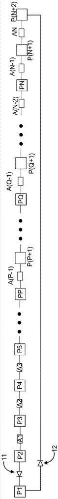
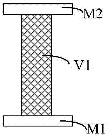
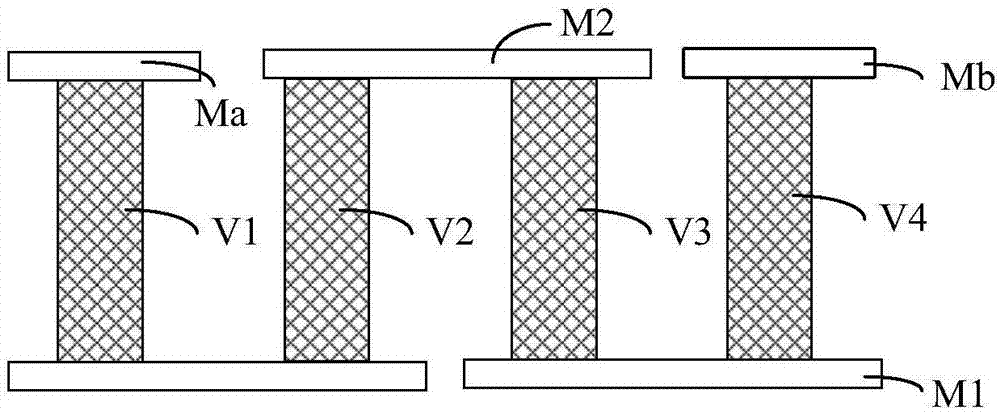
[0033] figure 1 is a schematic diagram of a semiconductor test structure according to an embodiment of the present invention. Figure 2 to Figure 4 yes figure 1 Schematic diagrams of cross-sectional structures of any three sub-test structures from the first sub-test structure, the second sub-test structure, ... to the Nth test structure.

[0034] The following combination Figure 1 to Figure 4 As shown, the semiconductor test structure provided by an embodiment of the present invention is introduced.

[0035] refer to figure 1 As shown, the test structure is formed in the dicing line (not shown) of the wafer, including:

[0036] The first welding pad P1, the second welding pad P2, the third welding pad P3, ..., the N+2th welding pad P...


PUM


Abstract

The invention provides a semiconductor testing structure and a stress migration testing method. A first welding pad, a second welding pad ...and an N+2 welding pad are arranged in a wafer cutting line along the cutting line extending direction. A sub testing structure required by stress migration tests is arranged between each two adjacent welding pads except the first welding pad and the second welding pad. During a testing process, a one-direction electric conduction structure arranged between the first welding pad and the second welding pad and a one-direction electric conduction structure arranged between the first welding pad and the N+2 welding pad enable a) a first testing path between the first welding pad and an P welding pad via the N+2 welding pad... to be in conduction in an alternative manner and resistance of N+1-P sub testing structures in the paths is acquired by using a Kelvin four-wire method; or b) a second testing path between the first welding pad to a Q welding pad via the second welding pad... to be in conduction and the resistance of the remained P-1 sub testing structure is acquired by adopting the Kelvin four-wire method, wherein Q>(P+1). By adopting the above structure, the floor occupancy of the testing structure provided by the invention is reduced and the testing efficiency is improved.

Description

technical field [0001] The invention relates to the technical field of semiconductors, in particular to a semiconductor testing structure and a stress migration testing method. Background technique [0002] During the manufacturing process of the integrated circuit, the stress-migration (Stress-Migration, SM) phenomenon of the metal interconnection layer, especially the conductive plug, causes the open circuit and short circuit of the metal interconnection structure, which increases the leakage current of the device. With the continuous expansion of the scale of integrated circuits, the continuous reduction of device size, the continuous reduction of the line width of metal interconnection lines, and the continuous increase of current density, it is more prone to failure due to stress migration, which has become an important reliability issue. [0003] Stress migration is a physical phenomenon that at a certain temperature, due to the different thermal expansion coefficients...

Claims


Application Information

Patent Timeline
Patent Type & Authority Applications(China)
IPC IPC(8): H01L23/544H01L21/60
CPCH01L23/544H01L22/34
Inventor 朱月芹宋永梁
Owner SEMICON MFG INT (SHANGHAI) CORP
Why Eureka
Try Eureka