Epitaxial wafer for gallium-nitride-based light emitting diode, and preparation method for epitaxial wafer

A light-emitting diode, gallium nitride-based technology, applied in the direction of electrical components, circuits, semiconductor devices, etc., can solve the problems of reducing the luminous efficiency of light-emitting diodes, and achieve the effects of improving energy band matching, increasing luminous efficiency, and enhancing electrical contact

Active Publication Date: 2017-06-20
HC SEMITEK ZHEJIANG CO LTD
View PDF4 Cites 8 Cited by
  • Summary
  • Abstract
  • Description
  • Claims
  • Application Information

AI Technical Summary

Problems solved by technology

[0006] In order to solve the problem of reducing the luminous efficiency of light-emitting diodes in the prior art, an embodiment o

Method used


Image

  • Epitaxial wafer for gallium-nitride-based light emitting diode, and preparation method for epitaxial wafer
  • Epitaxial wafer for gallium-nitride-based light emitting diode, and preparation method for epitaxial wafer

Examples


Embodiment 1

[0026] An embodiment of the present invention provides an epitaxial wafer of a gallium nitride-based light-emitting diode, see figure 1 , the epitaxial wafer includes a sapphire substrate 1, and a GaN buffer layer 2, an undoped GaN layer 3, an N-type GaN layer 4, a multiple quantum well layer 5, a P-type AlGaN layer 6, P-type layer 7.

[0027] In this embodiment, the P-type layer is formed by alternately stacking P-type GaN layers and graphene film layers.

[0028] Optionally, the thickness of the P-type GaN layer is 2-50nm, and adopting an appropriate thickness range can improve the transmission of activated holes and injection into the multi-quantum well layer, and reduce the loss of holes due to relaxation in the P-type GaN layer, The effective output of holes is improved, thereby increasing the number of holes injected into the multi-quantum well layer, and finally improving the luminous efficiency of the light-emitting diode.

[0029] Optionally, the number of graphene ...

Embodiment 2

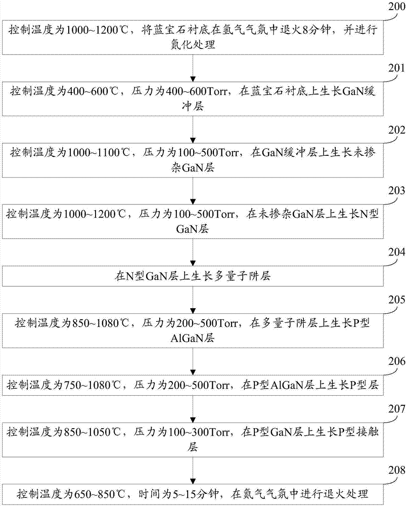
[0044] An embodiment of the present invention provides a method for preparing an epitaxial wafer of a gallium nitride-based light-emitting diode, which is suitable for preparing the epitaxial wafer provided in Embodiment 1. See figure 2 , the preparation method comprises:

[0045] Step 200: Control the temperature to 1000-1200° C., anneal the sapphire substrate in a hydrogen atmosphere for 8 minutes, and perform nitriding treatment.

[0046] Understandably, step 200 can clean the surface of the sapphire substrate.

[0047] In this embodiment, the sapphire substrate 1 adopts (0001) crystal orientation sapphire.

[0048] Step 201: Control the temperature to 400-600° C. and the pressure to 400-600 Torr to grow a GaN buffer layer on the sapphire substrate.

[0049] Optionally, the thickness of the GaN buffer layer may be 15-35 nm.

[0050] Optionally, after step 201, the preparation method may further include:

[0051] The control temperature is 1000-1200° C., the pressure is...


PUM

PropertyMeasurementUnit
Thicknessaaaaaaaaaa
Thicknessaaaaaaaaaa
Growth temperatureaaaaaaaaaa

Abstract

The invention discloses an epitaxial wafer for a gallium-nitride-based light emitting diode, and a preparation method for an epitaxial wafer, and belongs to the technical field of semiconductors. The epitaxial wafer comprises a sapphire substrate, a GaN buffering layer, a non-doped GaN layer, an N-type GaN layer, a multi-quantum-well layer, a P-type electron blocking layer and a P-type layer, wherein the GaN buffering layer, the non-doped GaN layer, the N-type GaN layer, the multi-quantum-well layer, the P-type electron blocking layer and the P-type layer are sequentially stacked on the sapphire substrate. The P-type layer is formed by the alternate stacking of a P-type GaN layer and a graphene film layer. According to the invention, the P-type GaN layer and the graphene film layer are alternately stacked to form the P-type layer, and the graphene film layer can prompt the hole transmission and also can improve the lateral extension capability of hole. Moreover, the graphene film layer also can improve the energy band matching of the P-type electron blocking layer and the P-type GaN layer, improves the electrical contact of the P-type electron blocking layer with the P-type GaN layer, improves the capability of a hole injection multi-quantum-well layer and finally improves the luminous efficiency of a light-emitting diode.

Description

technical field [0001] The invention relates to the technical field of semiconductors, in particular to an epitaxial wafer of a gallium nitride-based light-emitting diode and a preparation method thereof. Background technique [0002] Light Emitting Diode (English: Light Emitting Diode, LED for short) is a semiconductor device capable of effectively converting electrical energy into light energy. At present, gallium nitride-based LEDs have received more and more attention and research. [0003] The epitaxial wafer of a GaN-based LED includes a sapphire substrate, a GaN buffer layer, an undoped GaN layer, an N-type GaN layer, and a multiple quantum well layer (English: Multiple Quantum Well, referred to as: MQW) stacked on the sapphire substrate in sequence. , P-type AlGaN layer, and P-type GaN layer. When a current flows, the electrons in the N-type GaN layer and the holes in the P-type GaN layer enter the multi-quantum well layer to recombine and emit light. [0004] In t...

Claims


Application Information

Patent Timeline
IPC IPC(8): H01L33/00H01L33/06H01L33/32
CPCH01L33/007H01L33/06H01L33/325
Inventor 王群郭炳磊董彬忠李鹏王江波
Owner HC SEMITEK ZHEJIANG CO LTD
Why Eureka
Try Eureka