Low-capacitance TVS (transient voltage suppressor) diode and manufacture method thereof

A diode and low-capacitance technology, applied in the field of conductor chip manufacturing process, can solve the problems of increasing device manufacturing cost, large device area, large additional capacitance, etc., and achieve the effects of reducing device parasitic capacitance, small device area, and reducing manufacturing cost

Inactive Publication Date: 2017-06-27
罗灿
View PDF2 Cites 4 Cited by
  • Summary
  • Abstract
  • Description
  • Claims
  • Application Information

AI Technical Summary

Problems solved by technology

However, the additional capacitance introduced by these two structures is large, and the device area is large, which reduces the device performance and increases the device manufacturing cost.

Method used


Image

  • Low-capacitance TVS (transient voltage suppressor) diode and manufacture method thereof
  • Low-capacitance TVS (transient voltage suppressor) diode and manufacture method thereof
  • Low-capacitance TVS (transient voltage suppressor) diode and manufacture method thereof

Examples


Embodiment

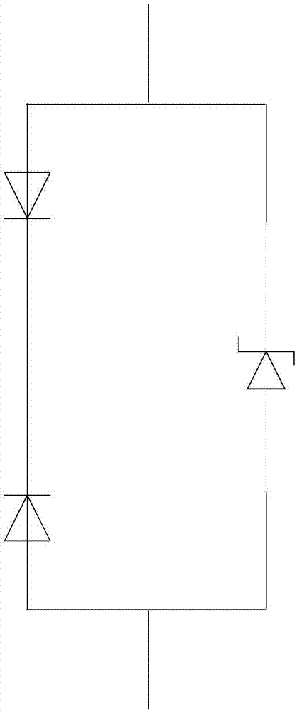
[0032] Embodiment: a kind of low electric capacity TVS diode and manufacturing method thereof, wherein the structure of this low electric capacity TVS diode is as Figure 10 As shown, its equivalent circuit diagram is shown in figure 1 shown.

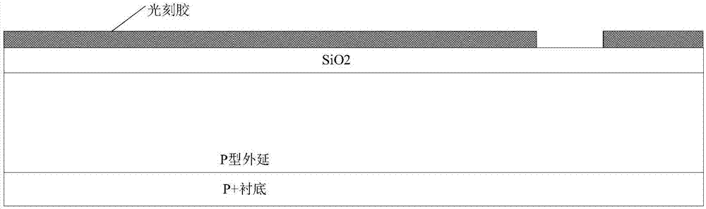
[0033] Including the back metal layer on the back side, the back metal layer is provided with a P+ substrate layer made of P-type silicon wafer, the P+ substrate layer is provided with a P-type epitaxial layer, the P-type epitaxial layer is provided with a dielectric layer, and the dielectric layer is provided with There is a front metal layer.

[0034] It also includes a first N-type implantation region, a second N-type implantation region and a first P-type implantation region.

[0035] The first N-type implantation region runs through the P-type epitaxial layer, and the first N-type implantation region is inserted into the P+ substrate layer, and the second N-type implantation region is inserted into the P-type epitaxial layer from...


PUM


Abstract

The invention discloses a low-capacitance TVS (transient voltage suppressor) diode and a manufacture method thereof; the low-capacitance TVS diode is characterized in that three TVSs are integrated and connected in parallel through process modifications based on traditional TVSs, parasitic capacitance of a device is reduced, the device has small area, the process has low difficulty, and device manufacturing cost is reduced; the modified TVS device has improved protective property and reliability.

Description

technical field [0001] The invention relates to the technical field of conductor chip manufacturing technology, more specifically, it relates to a low-capacitance TVS diode and a manufacturing method thereof. Background technique [0002] Transient Voltage Suppressor (TVS) is a solid-state semiconductor device specially designed to protect sensitive semiconductor devices from transient voltage surge damage. It has small clamping coefficient, small size, fast response, and leakage Due to the advantages of small current and high reliability, it has been widely used in voltage transient and surge protection. Electrostatic discharge (ESD), along with other random voltage transients in the form of voltage surges, are commonly found in a variety of electronic devices. As semiconductor devices are increasingly miniaturized, high-density, and multi-functional, electronic devices are increasingly vulnerable to voltage surges, which can even cause fatal injuries. Voltage surges rang...

Claims


Application Information

Patent Timeline
Patent Type & Authority Applications(China)
IPC IPC(8): H01L29/861H01L21/329
CPCH01L29/861H01L29/6609
Inventor 罗灿
Owner 罗灿
Why Eureka
Try Eureka