Frequency-adjustable microwave absorber
An absorber, microwave technology, applied in electrical components, antennas, magnetic field/electric field shielding and other directions, can solve the problem that the absorption frequency cannot be changed, and achieve the effect of convenient processing, light weight and good absorption effect
- Summary
- Abstract
- Description
- Claims
- Application Information
AI Technical Summary
Problems solved by technology
Method used
Image

Examples
Embodiment Construction
[0020] The present invention will be further described below in conjunction with the accompanying drawings.
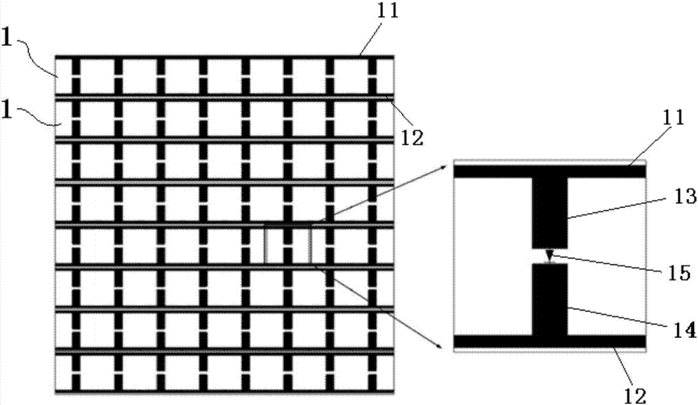
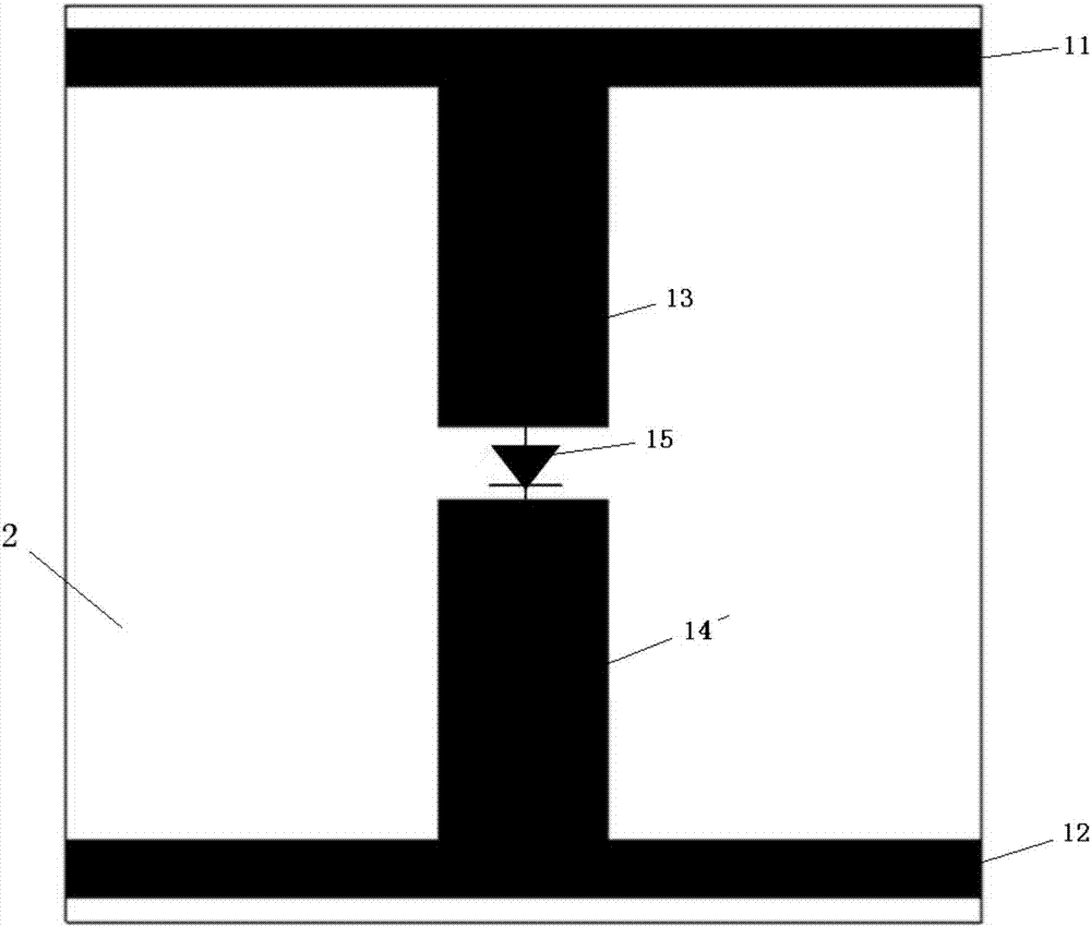
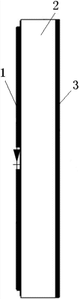
[0021] like Figure 1-Figure 3 As shown, a frequency-tunable microwave absorber includes: a resonant unit group 1, a dielectric substrate 2, and an anti-transmission layer 3. A plurality of resonant unit groups 1 are arranged on the top surface of the dielectric substrate 2 at intervals, and the dielectric substrate 2 An anti-transmission layer 3 is provided on the back; the resonant unit group 1 includes: a first metal bar 11 and a second metal bar 12, the first metal bar 11 and the second metal bar 12 are arranged in parallel, the second Between a metal horizontal bar 11 and the second metal horizontal bar 12, multiple groups of first metal vertical bars 13 and second metal vertical bars 14 are arranged oppositely, each group of first metal vertical bars 13 and second metal vertical bars The ends of the strips 14 are connected via varactor diodes 15 .
[0022] Each...
PUM
| Property | Measurement | Unit |
|---|---|---|
| Thickness | aaaaa | aaaaa |
Abstract
Description
Claims
Application Information
PatSnap Eureka turns technology decisions into work you can execute. Powered by our Innovation Knowledge Graph, it runs expert workflows across engineering, life sciences, materials and intellectual property. Get your review-ready output in minutes.


