Exposure system and exposure method used for semiconductor lithography

A technology of exposure system and exposure method, which is applied in the field of semiconductor lithography, can solve the problems of low realizability and reliability of the exposure system, dynamic disturbance of the optical system, complex system structure, etc., so as to improve the realizability and reliability, Effect of avoiding mechanical vibration and reducing complexity

Active Publication Date: 2017-07-07
SHANGHAI MICRO ELECTRONICS EQUIP (GRP) CO LTD
View PDF6 Cites 5 Cited by
  • Summary
  • Abstract
  • Description
  • Claims
  • Application Information

AI Technical Summary

Problems solved by technology

[0003] The traditional variable slit is realized by the high-speed and high-acceleration motion of the knife-edge mechanical structure. It is necessary to design a physical motion with a high acceleration of 5-10G in the exposure system, which introduces a large dynamic disturbance to the precise optical system and affects the final lighting performance
At the same time, in order to realize the correction of non-scanning and high-order dose errors in the field, the variable slit of the traditional structure needs to make nearly 20 pairs of programmable micro-motion structures on the knife edge, resulting in an extremely complex system structure, and the variable slit It is a mechanical device, which will inevitably produce vibration and shock during the change process, and the change also requires the driving system of the variable slit to have a high acceleration function, which makes the engineering feasibility and reliability of the entire exposure system low

Method used


Image

  • Exposure system and exposure method used for semiconductor lithography
  • Exposure system and exposure method used for semiconductor lithography
  • Exposure system and exposure method used for semiconductor lithography

Examples


Embodiment Construction

[0025] In order to make the above objects, features and advantages of the present invention more comprehensible, specific implementations of the present invention will be described in detail below in conjunction with the accompanying drawings.

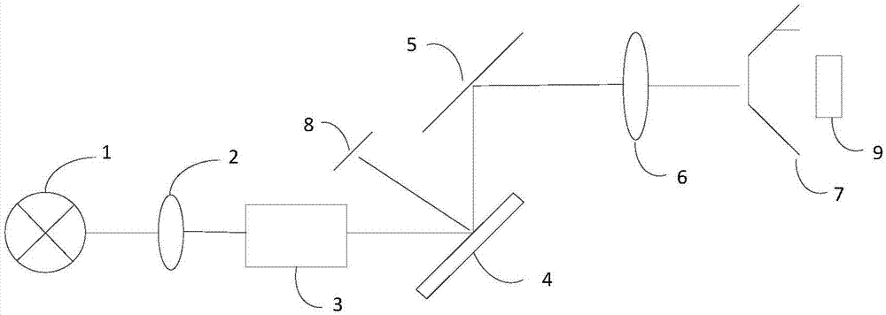
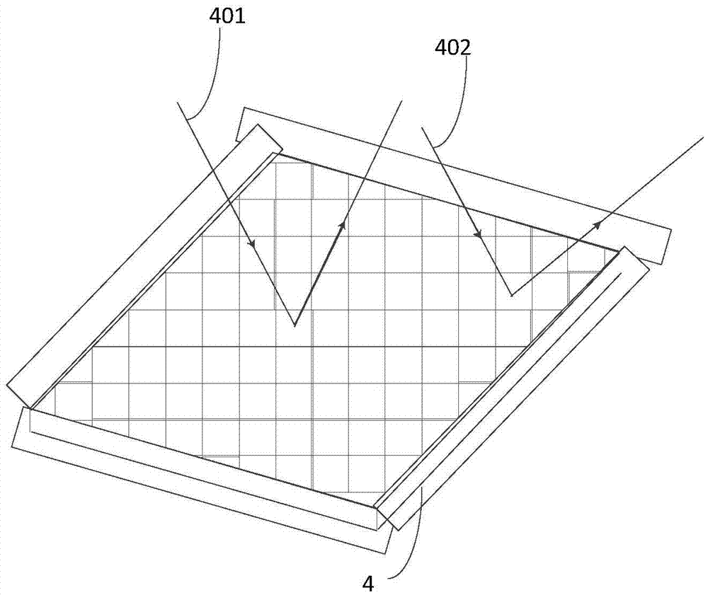
[0026] Please refer to figure 1 The exposure system provided by the present invention sequentially includes an illumination light source 1, a collimator beam expander system 2, a uniform light unit 3, a microreflector array 4, a reflector 5, a relay unit 6, a mask template 7 and a workpiece table 9, A light absorbing device 8 is also arranged between the uniform light unit 3 and the reflector 5, so that the light emitted from the illumination source 1 passes through the quasi-beam expander system 2 and the uniform light unit 3 in sequence and then is transmitted to the micromirror array 4 , the micromirror array 4 reflects the required light beams to the mirror 5, and then is transmitted to the mask plate 7 and the workpiece stage 9 th...


PUM


Abstract

The invention discloses an exposure system and an exposure method used for semiconductor lithography. A micro reflector array is arranged between a light-homogenizing unit and a reflector to replace a conventional variable slit apparatus; parameters of an exposure field of view are set according to mask plate patterns and exposure precision in exposure, and the parameters are input to driving software of the micro reflector array; the movement parameters of the micro reflector array in exposure are calculated; in exposure, a control board card continuously transmits an instruction to each digital micromirror in the micro reflector according to data in the driving software; and each digital micromirror performs a corresponding turnover action after the instruction is received at each moment until exposure is finished. The micro reflector array adopted by the exposure system and the exposure method comprises tens of thousands of digital micro mirrors which can change exposure field of view, range and dosage in real time, so that the mechanical vibration generated by the conventional variable slit apparatus in changing slit shapes and high acceleration speed requirement of the driving system of the variable slit apparatus are avoided; and therefore, the complexity of the mechanical structure and the control system of the exposure system is lowered.

Description

technical field [0001] The invention relates to the field of semiconductor lithography, in particular to an exposure system and an exposure method for semiconductor lithography. Background technique [0002] In the semiconductor IC integrated circuit manufacturing process, a complete chip usually needs to undergo multiple lithography exposures to complete, and the mask used for each lithography and process requirements will change. When the process requirements are high , the light intensity needs to be concentrated and the stray light needs to be blocked. When the pattern area of ​​the mask is complex, the invalid stray light in some areas also needs to be blocked to ensure the accuracy of the pattern left on the silicon wafer after exposure. However, when the process requirements are relatively low, or the graphic area is relatively simple, and the lithography precision requirements are low, the part of the stray light with low light intensity generated by the illumination...

Claims


Application Information

Patent Timeline
Patent Type & Authority Applications(China)
IPC IPC(8): G03F7/20
CPCG03F7/2008G02B26/08G03F7/20
Inventor 葛亮杨志勇
Owner SHANGHAI MICRO ELECTRONICS EQUIP (GRP) CO LTD
Why Eureka
Try Eureka