
Chip verification method, device and system

A chip and verification platform technology, applied in the communication field, can solve the problems of lack of hierarchy in the verification architecture and low platform reusability, and achieve the effect of improving reusability and verification efficiency

Active Publication Date: 2020-11-03
ZTE CORP
View PDF12 Cites 0 Cited by
  • Summary
  • Abstract
  • Description
  • Claims
  • Application Information

AI Technical Summary

Problems solved by technology

[0007] The present invention provides a chip verification method, device and system to at least solve the problem of low reusability of the platform due to the lack of hierarchy of UVM verification architecture

Method used


Image

  • Chip verification method, device and system
  • Chip verification method, device and system
  • Chip verification method, device and system

Examples


Embodiment Construction

[0030] Hereinafter, the present invention will be described in detail with reference to the drawings and examples. It should be noted that, in the case of no conflict, the embodiments in the present application and the features in the embodiments can be combined with each other.

[0031] It should be noted that the terms "first" and "second" in the description and claims of the present invention and the above drawings are used to distinguish similar objects, but not necessarily used to describe a specific sequence or sequence.

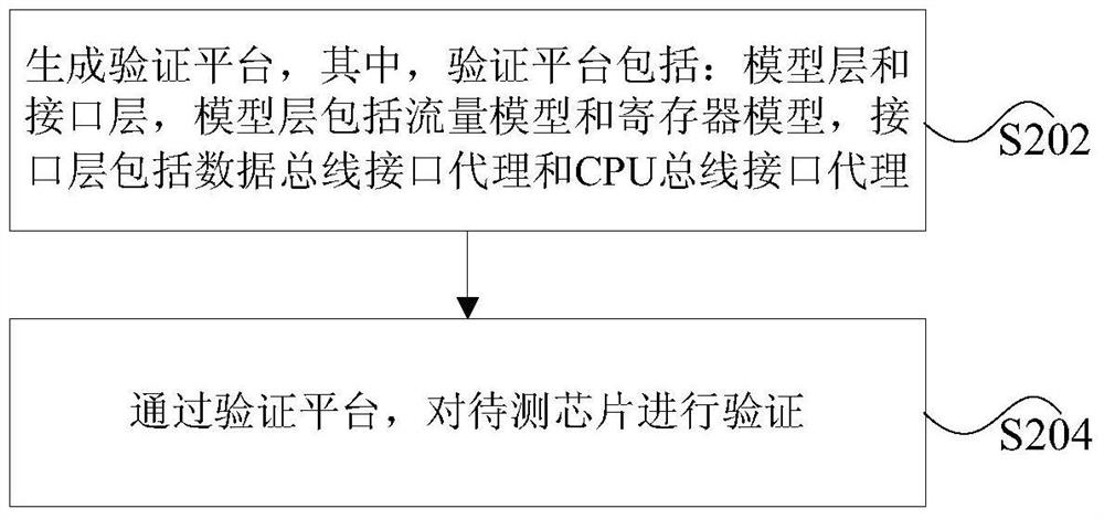
[0032] In this embodiment, a chip verification method is provided, figure 2 is a flowchart of a chip verification method according to an embodiment of the present invention, such as figure 2 As shown, the process includes the following steps:

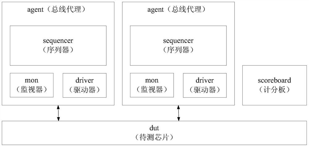
[0033] Step S202, generating a verification platform, wherein the verification platform includes: a model layer and an interface layer, the model layer includes a traffic model and a register model, and the ...


PUM


Abstract

A chip verification method, comprising: generation of a verification platform, the verification platform comprising: a modeling layer and an interface layer, the modeling layer comprising a flow model and a register model, and the interface layer comprising a data bus interface agent and a CPU bus interface agent; verification of chips to be tested is carried out by means of the verification platform. The described technical solution resolves the problem of low reusability in verification structures due to the lack of hierarchy in same, thus increasing the reusability of verification structures and enhancing verification efficiency.

Description

technical field [0001] The present invention relates to the communication field, in particular to a chip verification method, device and system. Background technique [0002] Logic verification is a key step in the front-end design process of digital chips. It verifies the actual operating environment of the platform simulation chip and verifies the correctness of the chip functions through test cases. With the rapid growth of digital integrated circuits in scale and complexity, and the rapid release of a large number of similar-function chips, higher requirements are placed on verification platforms and test methods in terms of time and cost. [0003] The traditional verification platform is the verification of the signal level, and the chip under test is verified by directly writing the test stimulus. The traditional verification platform lacks an abstract division of labor for platform functions, and there is no unified writing standard and application interface, resulti...

Claims


Application Information

Patent Timeline
Patent Type & Authority Patents(China)
IPC IPC(8): G01R31/317G01R31/3177
CPCG01R31/31718G01R31/3177G06F30/00
Inventor 朱仁霖
Owner ZTE CORP
Learn More